This thread has been locked.

If you have a related question, please click the "Ask a related question" button in the top right corner. The newly created question will be automatically linked to this question.

UCC28070: Question about VDS ringing

Guru 19485 points
Part Number: UCC28070

One customer is designing UCC28070 on 2.3kW (390V / 5.9A) function. 

※Input is 200Vac

But problem is occurring, Vds ringing is large.

My question is two points below, please let me know any advice;

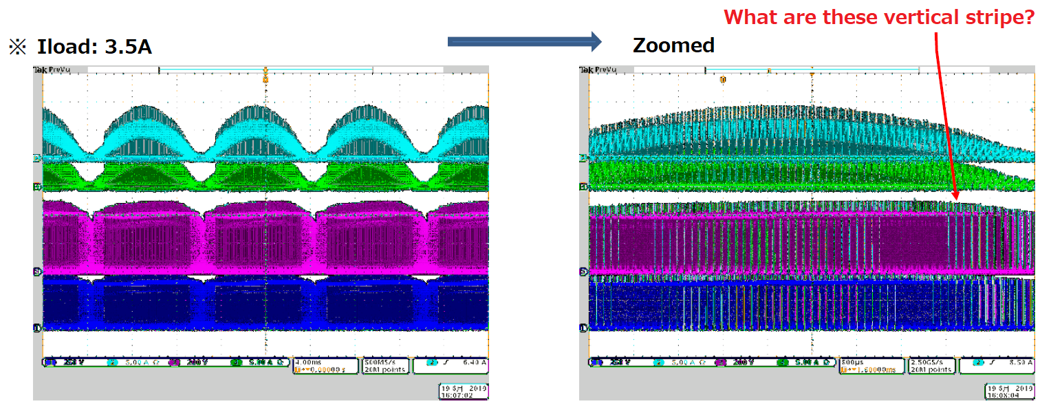
①When load current increase to "0A → 0.5A → 1A → --- → 5.9A" and measure by oscilloscope, waveform is conspicuous vertical stripe.

 What is the reason of below vertical stripe?

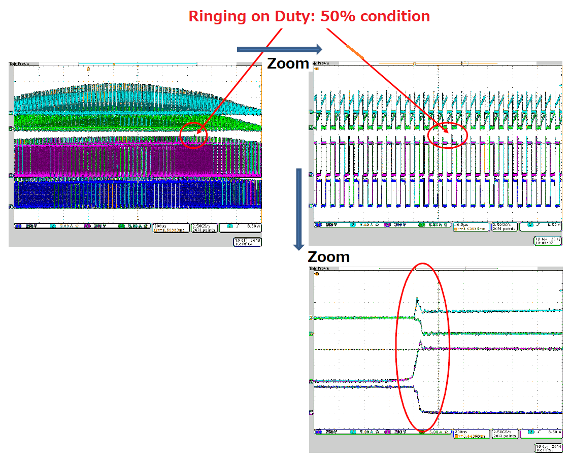
②When timing for duty cycle exceed 50% (Less than 50% → 50%), large VDS ringing is occur and larger current become more large VDS ringing.

 ※In the case of "over 50% → less than 50%" is no problem.

 Please let me know about the reason of increase VDS ringing by over 50% duty.

  And, is there any idea for reduce ringing?

Best regards,

Satoshi

  • Hello Satoshi-san

    The 'Vertical stripes' are almost certainly an artifact caused by the 'scope screen resolution. One way to check this would be to split the screen and look at one of the stripes using the zoom function.

    The ringing at 50% duty cycle is probably due to some interaction between the turn-off of one MOSFET and the turn-on of the other. The PCB layout may have an effect on this but I really couldn't give any specific advice without seeing the PCB Gerber files.

    The designers can check that this is what is happening by turning one of the PFC channels off. The easiest way to do this is to simply disconnect the gate drive resistor at one of the MOSFETs and tie its gate to the source.

    Regards
    Colin

  • Colin-san

    Thank you for reply,

    Customer information and additional question is below, please let me know any advice;

    【Customer information】

    ・Customer is not use circuit board and connecting only 1.25sq cable. 

     GND reference is tied Cout negative side (EL capacitor) of 380V output side.

     Each MOSFET's(source) are tied GND of AC input side.

    ・Rectifier Diode changed FRD to SiC, result was the same. (Customer guess that reason is recovery time)   

    ・Voltage source is; IC and FET driver's Vcc are independent VDC source, negative pin are also connect to negative source. 

      These line are connect to FET source.

     ※Because above connection become to reduce gate noise.

    ・First half of half-sine wave is not occur ringing.

    【Additional question】

    ①Is these happening mean interference, correct?

     Is there detailed application note for principle of interference (or ringing)? 

    ②Customer guess that gate's pull out if fast, or Vout become 380V to 430V for a moment.

     Is this time possible to drop inductance by interference?

    ③Anew, if there any idea for reduce ringing, please let me know.

    Best regards,

    Satoshi

  • Hello satoshi-san

    If the interference is happening only at the 50% duty cycle point then I would strongly suspect that there is an issue with the layout. The customer comment that "GND reference is tied Cout negative side (EL capacitor) of 380V output side and Each MOSFET's(source) are tied GND of AC input side." means that any inductance in the path from Cout Negative to MOSFET source will develop a voltage as the current is switched on and off. There is a PCB layout video at https://training.ti.com/pcb-layout-smps-part-1-2?cu=1134585. At about 7min 30s into the video there is a slide showing the switched current flowing in the O/P loop. Any stray inductance in this path will generate voltages as the current is turned on and off and the inductance of the input and output loops should be minimised.

    Any PCB related ringing  should be present on both the first half and second half of the line voltage sine wave and I don't know why that would be.

    The output output capacitor will prevent the output voltage of the PFC stage from increasing.

    If the customer would send me their schematic and PCB layout files (Gerber or original files please) I can review them. You may send them to me directly at colingillmor@ti.com They will of course remain confidential

    Regards

    Colin

  • Colin-san

    Thank you for reply,

    I requesting to customer for Layout information again, I will feedback to your mail if there any update from customer.

    I didn't look your attached picture below, could you attach picture again?

    Best regards,

    Satoshi

  • Hello Satoshi-san

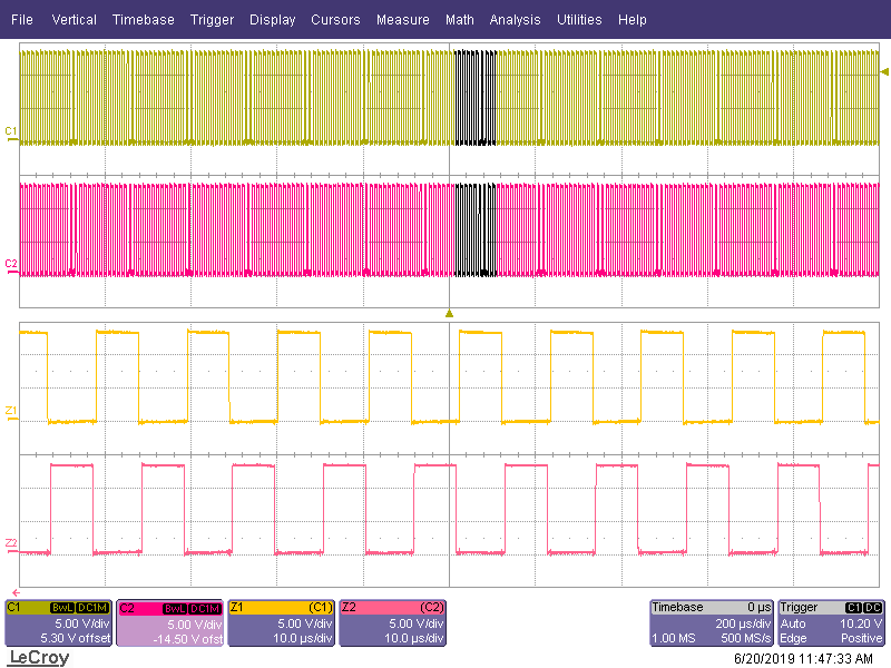
    Here it is - please let me know if it is not visible. I can see it right now as I type but I can never be sure that what I see is what gets posted.

    Regards
    Colin

  • Hello Satoshi-san

    I's been a while since this thread was updated so I'm going to close it now but please feel free to open a new one if there are any further questions about this or any other project.

    Regards
    Colin