This thread has been locked.

If you have a related question, please click the "Ask a related question" button in the top right corner. The newly created question will be automatically linked to this question.

BQ51013B: Design and Schematic Review Requested for Wireless Project

Part Number: BQ51013B
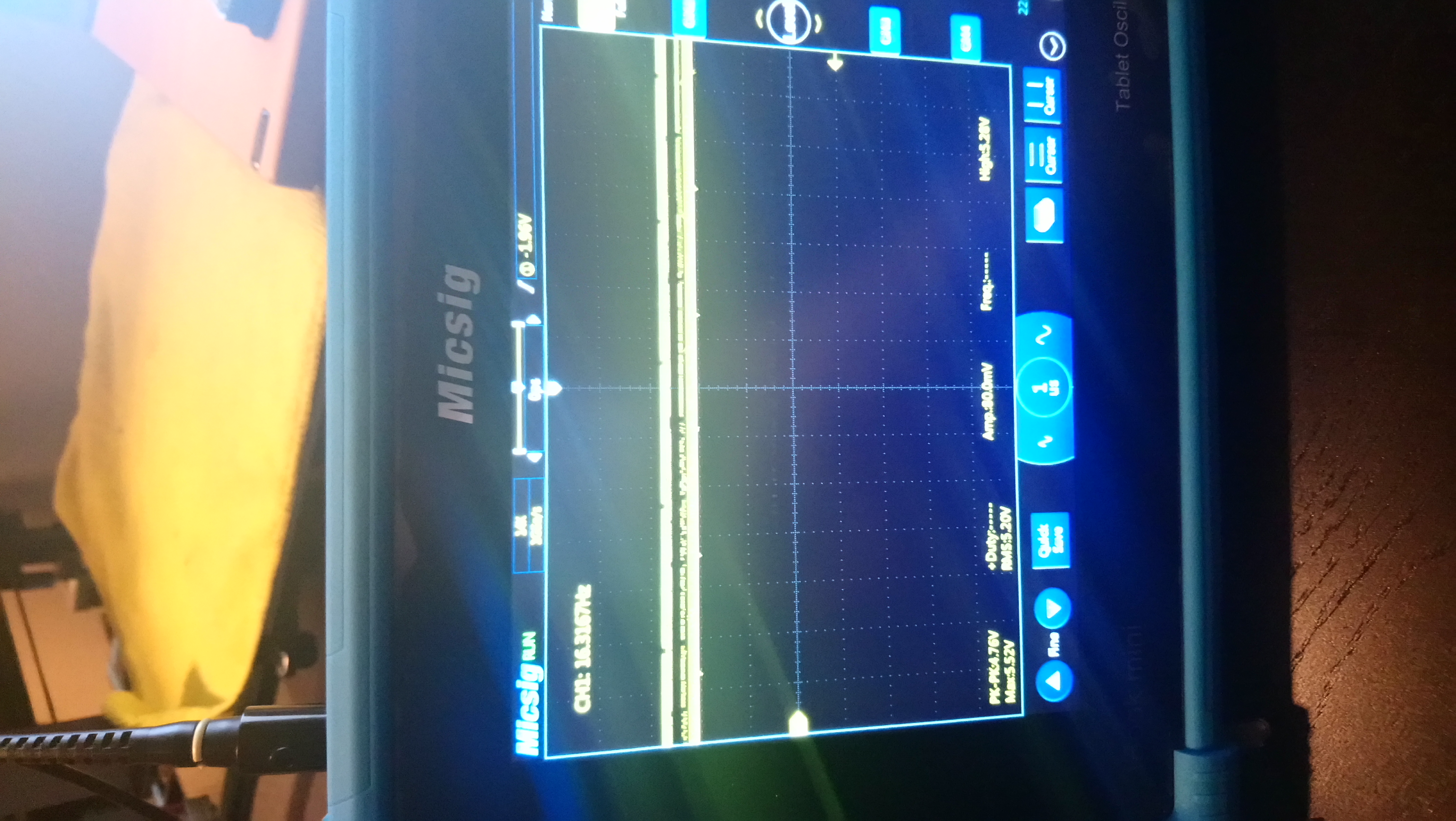
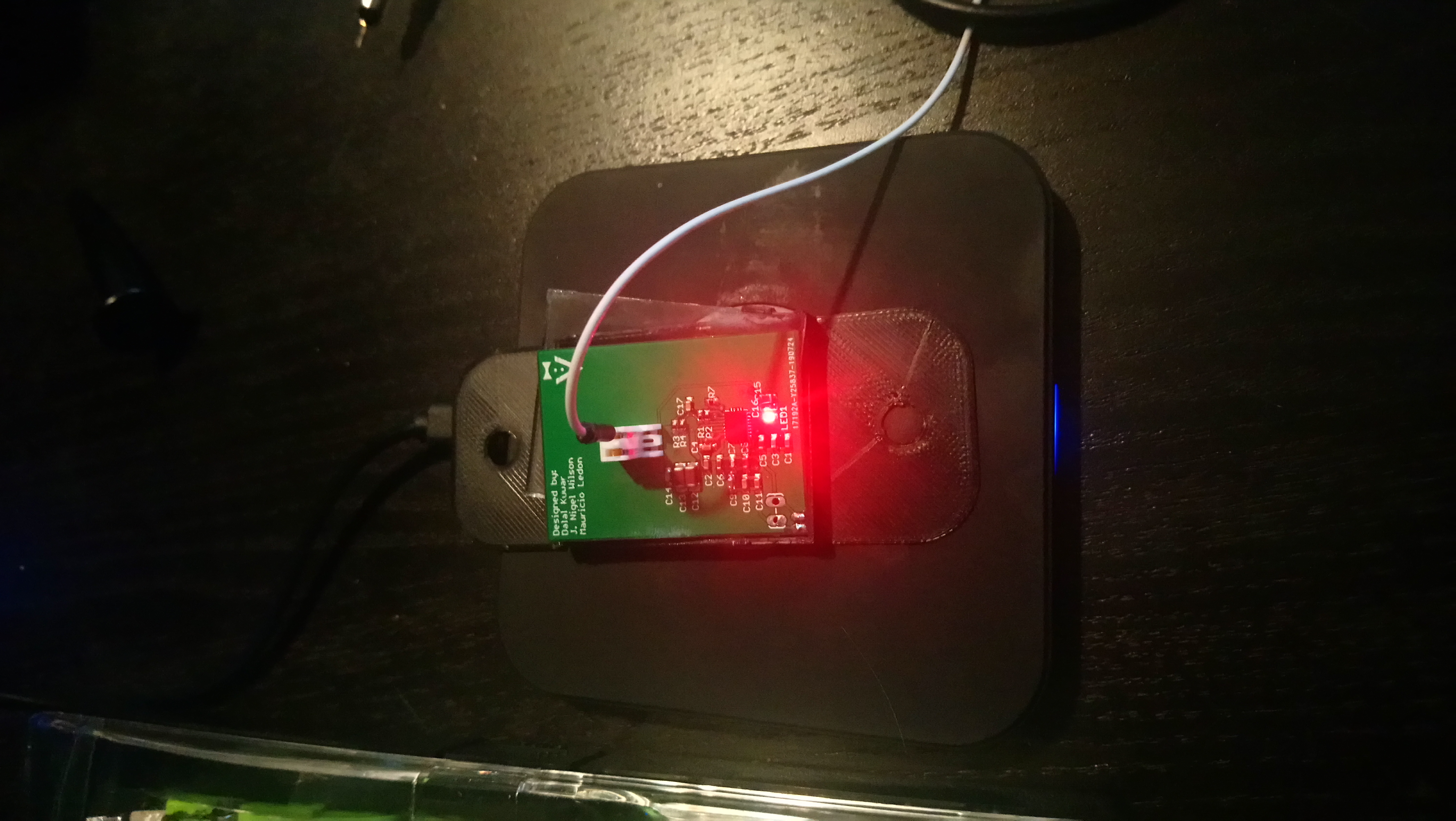
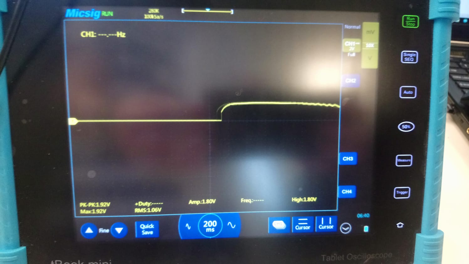
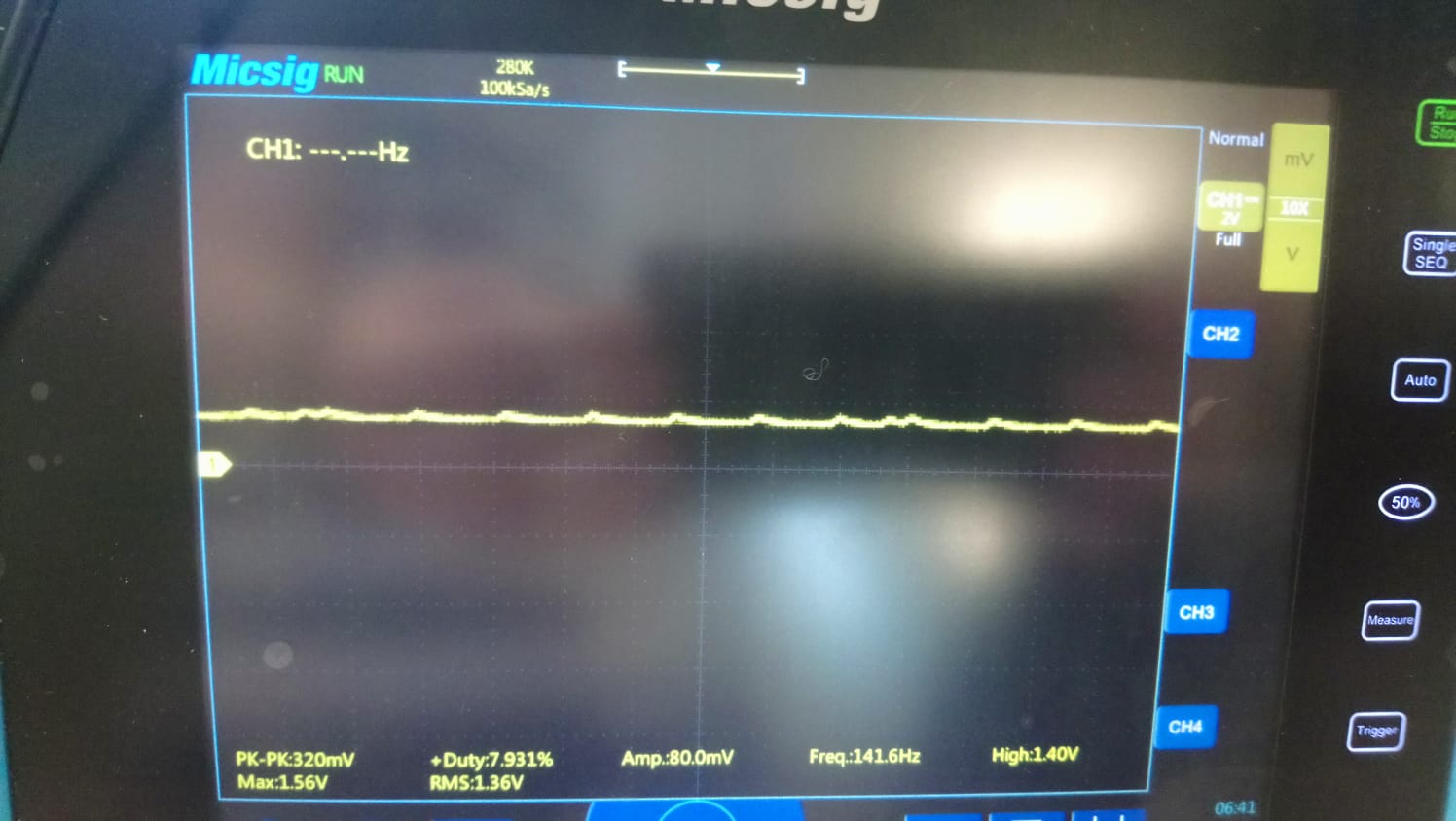
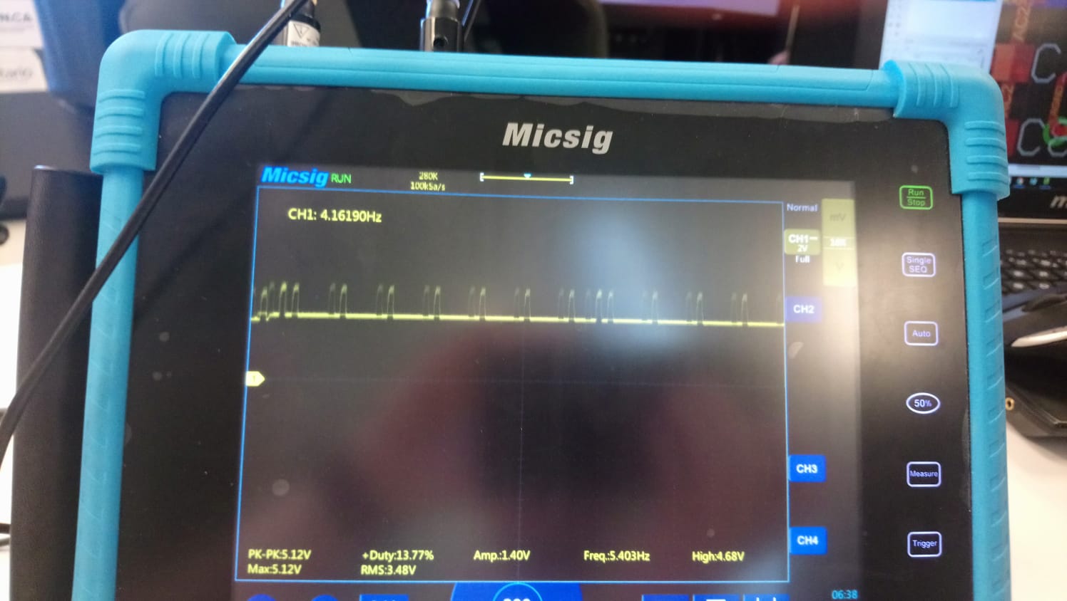
Hi guys. I am part of a college engineering team developing a product that utilizes TI's BQ51013B chip to provide a wireless charging solution. The application requires charging of two lithium Ion 14430 batteries of 600 mA each and they both draw about 300-500 mA.
I am having difficulty sizing the comm/boot capacitors exactly for our application. We are using a coil with the following characteristics:

Inductance +/-2%, @ 200kHz (uH) = 11.6
DCR +/- 2% (mOhm) = 520
ESR +/- 2%(mOhm) = 635
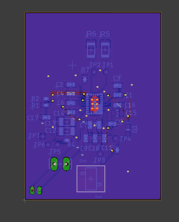
Q Factor = 23ProjectSchematic.pdf

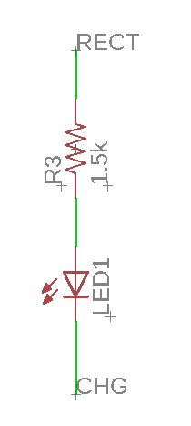
I have attached a schematic as a pdf format based on the Datasheet. I would appreciate any feedback and review. 

An important question I had is how far can the coil be placed from the chip itself and is it possible to place it at a longer distance of about 10-15 cms somehow?

  • Hello

    10cm to 15cm is a little too far for this system.  Typical coil to coil distance is 3mm to 5mm. 

    The TX sends out a digital ping, this is full wave rectified to produce a voltage at RECT pin.  The voltage needs to exceed UVLO 2.7V to start operation.

    Schematic looks OK.

  • Thank you very much for your prompt assistance Bill. I will try this out.

    Sincerely,

    Kuwar Dalal

    Electrical Engineering Technologist

    Applied Research Division

    Algonquin College, Ottawa Ontario

  • Hi Bill,

    Our PCB's arrived and we tested them. They seem to be recognized by transmitters but the output voltage of the board is just under 1.7 volts. Would there possibly any specific reason for this? How would I go about testing/diagnosing the problem?

    Thanks for you time.

    Kuwar Dalal

  • Hi Kuwar

    Are you seeing the 1.7V at RECT pin?

    This is an indication the coupling and gain of coil is low, possibly tuning is an issue.

  • I will check the voltage on the RECT pin and get back ASAP. I was only able to 1.7 on the OUT pin. I also just noticed that I put the RECT capacitor C3 after the Ros resistor. Could that possibly be an issue? 

  • Is the capacitor C3 or C17?   C17 in above schematic is not a problem.  But you do need a large bulk capacitor on RECT pin.

    It is odd that you are getting 1.7V on OUT.  The output is not enabled until the voltage on RECT is at target.

  • I misread my schematic, I do have a bulk capacitor as the datashet recommends on C3.

    I did some further tests today. I chose a random qi wireless transmitter and measured voltages at each pin with strange results. The signal across the coil looks like this: 

    A close up looks like this: 

    The Voltage at the Rect pin is between 3.5 volts to 5.5 volts sometimes and looks like this:

    The voltage on the output is still between 1.4 to 1.8 volts although I did get 2 volts fiddling with the placement. The PCB looks like this:

  • We are using the following receiver coil:  https://www.digikey.ca/product-detail/en/molex/1461791001/WM15000-ND/6159262

    I have to try different coils to see if anything else works. The datasheet walks through the calculation of C1 and C2 for tuning and says " For this application, the selected coil inductance, Ls, is 11 μH and the Ls' is 16 μH with a DC resistance of 191 mΩ." What coil is used here that its referring to. Could this still be a gain/tuning issue?

    Appreciate all the help Bill!

    Respectfully,

    Kuwar Dalal

  • Hi Kuwar

    The Coil and tuning look OK.

    Can you take closer look at RECT voltage vs OUT voltage.  Should see the control packets at start up and during power transfer.

    What load are you testing with?

  • Hi Bill,

    "What load are you testing with?"

    I tried with just a plain red LED which seems to light up intermittently. I am seeing decent gain and coupling in the coil, so the tuning did seem OK. 

    I also noticed that I tied the LED to the RECT pin instead of the out pin but this wouldn't cause an issue like this would it?

     From the test and troubleshoot manual from TI I was able to find the following:

    I am only getting about 5 volts at the RECT. I tried some other coils as well. 

    The following pictures are form the scope:

    Vout on Start up:

    Vrect on startup:

    What could cause the voltage on Vrect pin to not be sufficient?

  • Hi Kuwar,

    I think may has some issue at your PCB layout.From your PCBA picture, the C14 & C16 are far from the BQIC, it is not good placement. you can reference "Layout Guidelines" in DS.

    Regards,

    Driscoll

  • Hi Driscoll,

    Thank you so much for your prompt reply. I could send you a pdf of our pcb layout. The C14 AND C 16 are just output capacitors meant to smooth out the Rect and out voltages. I didn't think this might have that much of an effect on the system. In fact after extensive troubleshooting yesterday our design even matches some off the shelf chargers by samsung and adafruit etc. Only difference being current output, we have 1 amp, the others are only configured for 500-600 ma. Here is some weird:

    I tried multiple coils with this design and multiple off the shelf chargers as well. They all seem the behave the same way.

    The coils are all recognized and transmitter transmits power, I can see the comm packets on the Rect output as the manual shows. However, the transmitter is only transmitting at roughly 10 volts pk to pk which our receiver sees. This is done at 144-146 kHz constantly. This signal is common across RX and TX coils. When this signal is rectified internally etc. It becomes 4.5 volts at the Rect pin and consequently only 1.8 bolts on the Out pin.

    When I tried a different off the shelf Samsung Receiver based on this chip with a design matching us, with minor differences in capacitance values about 10 NF we see that the transmitter transmits at 20 volts pk to pk. This is why the capacitors should be sized for 25 v minimum.

    From my understanding (I could be totally wrong here), the internal DRC (dynamic rectifier control) is supposed to send error packets to the TX to increase voltage until the output is at par. This does not seem to be happening.

    How would we even go about correcting/compensating something like this. It's really odd that communication and power contracts are established but the output is stuck at less that 2 volts.

  • We are working on this problem off line and making good progress.

    I will close this post for now, if needed we can open it later.

  • Hi Kuwar,

    I have encountered this situation like this.It is strongly recommended to modify the high frequency capacitor (C14) position of RECT.

    As close as possible to BQ51013B.

    Regards,

    Driscoll

  • Hi Driscoll,

    Thank You So much for your input and experience. Designing something like this especially high frequency circuits is new to me. Please check my attached schematic and pcb, we are about to get them manufactured. I have moved all elements much closer to the chip except for resistors/leds/thermistor. I have also added more Vias connected to ground (not shown in pcb above) to add shorter current loops back to the chip upon Bill's suggestion.

    Leaving En1 and En2 as floats/test points wouldn't be a problem would it?

    Final PCB receiver.pdfFinal Schematic Receiver.pdf

  • Hi Kuwar,

    1. Does your BQIC get a little hot when Vout around 2.5V at your original design?

    2. Suggest add 10 Kohm pull down to ground at EN1/ EN2 when don't controll by MCU; and just DNI for future design.

    3. Change  position C14 to C12, let C14 more closely to BQ51013B.

    4. How about contact resister of JP1?

    5. The power trace need as width as possible.

    6. the power path (AC2) should JP1 to C7/C8 to BQIC, should not JP1 to C7/C8/ BQIC, you can reference EVM.

    7. Vias seems not enough in your power path.

    Regards,

    Driscoll

  • Hey Driscoll,

    1. Does your BQIC get a little hot when Vout around 2.5V at your original design?

    No it does not get hot at all, I checked a few times.

    2. Suggest add 10 Kohm pull down to ground at EN1/ EN2 when don't controll by MCU; and just DNI for future design.

    EN1 and EN2 have internal pulldown resistors but I will add 10Kohm just in case

    3. Change  position C14 to C12, let C14 more closely to BQ51013B.

    Done. 

    4. How about contact resister of JP1?

    Jp1 is just where the coil would go, I put to spots for 2 different coils we were testing with

    5. The power trace need as width as possible.

    Done power trace is 0.254 mm.

    6. the power path (AC2) should JP1 to C7/C8 to BQIC, should not JP1 to C7/C8/ BQIC, you can reference EVM.

    I think I understand this and its fixed now.

    7. Vias seems not enough in your power path.

    Corrected and added multiple paths. 

    Please check attached files and let me know if you can notice anything else. Thank you so much again!

    Best regards,

    Kuwar DalalReceiver no Ground.pdf

    Receiver with Ground.pdf

  • Also what thickness PCB's do would you recommend for this. I got 1.6 mm last time.

  • Hi Kuwar,

    The 1.6mm thickness of PCB is okay for me. but power trace is 0.254 mm should not enough.

    BTW, your thermal copper under BQIC is not good enough, pls reference EVM.

    pls reference DS (page36).

    For a 1-A fast charge current application, the current rating for each net is as follows:

    • AC1 = AC2 = 1.2 A

    • OUT = 1 A

    • RECT = 100 mA (RMS)

    • COMMx = 300 mA

    • CLAMPx = 500 mA

    • All others can be rated for 10 mA or less

    others could check with Bill's suggestions.

    Regards,

    Driscoll

  • Thank you so much Driscoll,

    I will make all recommended changes in reference with the EVM. Will let you know if the next version works. Thanks again!