This thread has been locked.

If you have a related question, please click the "Ask a related question" button in the top right corner. The newly created question will be automatically linked to this question.

UCC21520: OUTB to VSSB pin short

Part Number: UCC21520

Hi all,

Refer this thread for  design details:

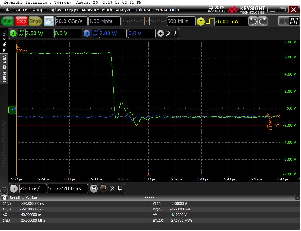
Recently we are seeing the failure in gate driver IC UCC21520.

Failure condition: OUTB to VSSB impedance short.

What would be the reason for above failure condition?

The module is worked for a month and after that failed during start up itself.

Refer attachment for schematics.Expecting  your valuable reply.

WIth regards,

P.Selvam.GAN driver section.pdf

  • Hi,

    Thank you for your question. I work on the applications team in the high power drivers group.

    Could you please confirm if you are using UCC21520A or UCC21520? Could you please specify which driver has failed, U12 or U18? Can you please provide what GaN FETs are being used for U104, U105, Q106, Q108, Q109, and Q110? Did anything else fail, or just the gate driver?

    Do you have any waveforms showing the gate driver outputs during start-up? I’m worried that the input voltage to the drivers might sag under high load and cause the device to drop below its UVLO falling threshold, especially on U12.

    Looking forward to your response.

    Thanks and best regards,

    John

  • Hi,

    Thank you for your reply.

    1.We are using UCC21520A

    2.GS66516T is used as GAN FET for all.

    3.GAN FET U104 and U105 also failed.

    4.Gate driver output node waveform measured at FET gate node and Switch node.Refer attachment:Blue waveform:U105(Vgs),Green waveform:Switch node.

    5.Input voltage sag in VCCI or VDDA or VDDB?

    Awaiting for your reply.

    With regards,

    P.Selvam

  • Hi Selvam,

    I’m talking about potential input voltage sag of VDDA of U12, which looks to be powered from a 6V rail of U11, which is under the recommended operating voltage of 6.5V. The driver could potentially drop below its UVLO falling threshold (5.7V typ) and cause errors in the system.

    It also appears that the -1.8V rail of U12, VSSB (pin 9) still needs to be locally decoupled with a small capacitor.

    What is the slew rate of the rising and falling edges of your switch node waveform?

    Can you please take a scope capture from OUT to VSS while switching? Our drivers have an abs. max of -2V for 200ns, and undershoots beyond this could potentially cause damage. It is important to mitigate this undershoot by correctly sizing gate resistors and ferrite beads.

    Thanks and best regards,

    John

  • 1.I’m talking about potential input voltage sag of VDDA of U12, which looks to be powered from a 6V rail of U11, which is under the recommended operating voltage of 6.5V. The driver could potentially drop below its UVLO falling threshold (5.7V typ) and cause errors in the system.

    VDDA voltage is 6.5V(LDO regulated supply).So,this won,t be probelm right.

    2.What is the slew rate of the rising and falling edges of your switch node waveform?

    Since its a resonant converter.SW node slew rate depends on resonant current.It will vary from 5ns to 30ns based on load.

    3.What is the slew rate of the rising and falling edges of your switch node waveform?

    Refer the attachment..Green:OUTB,Blue:VSSB(-1V)

    Thank you for your response.

    Revert back for any clarification.

    With regards,

    P.Selvam

  • Hi Selvam,

    Do you have any scope captures of the outputs and switch node during start-up? Start-up is usually more stressful to the system since there is no circulating current.

    Also, could you please share some pictures of your layout?

    Also, the ringing on your gates at these two points looks very large, is there any way you could increase your ferrite bead value to help mitigate stress seen by the driver?

    Looking forward to your response.

    Thanks,

    John