This thread has been locked.

If you have a related question, please click the "Ask a related question" button in the top right corner. The newly created question will be automatically linked to this question.

WEBENCH® Tools/UCC28C43: UCC28C43

Part Number: UCC28C43
Other Parts Discussed in Thread: LMV431

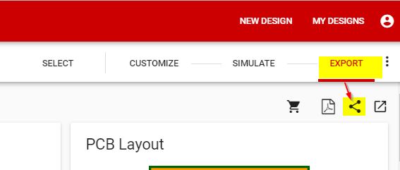
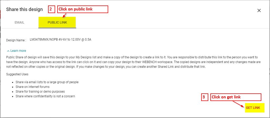
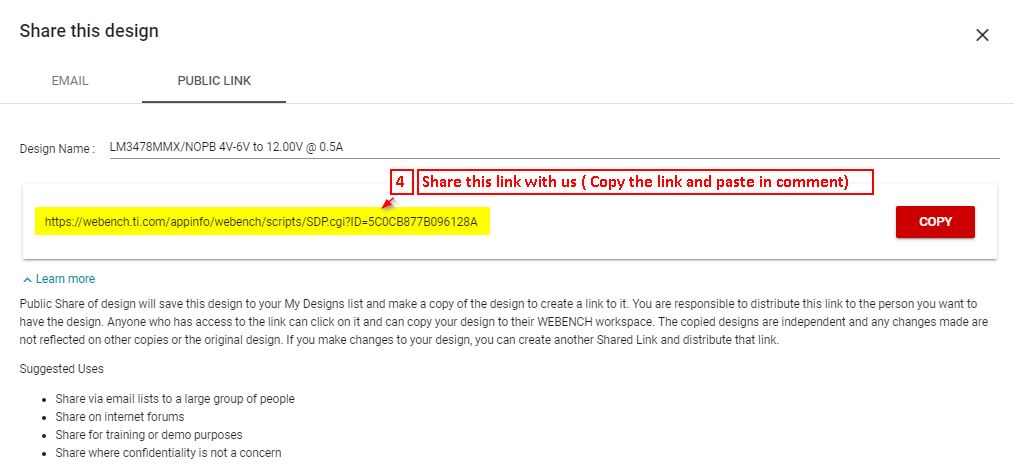
Tool/software: WEBENCH® Design Tools

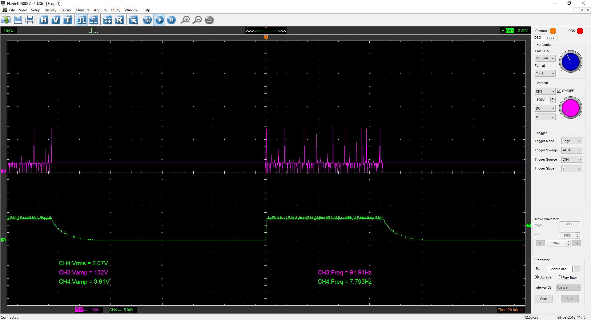
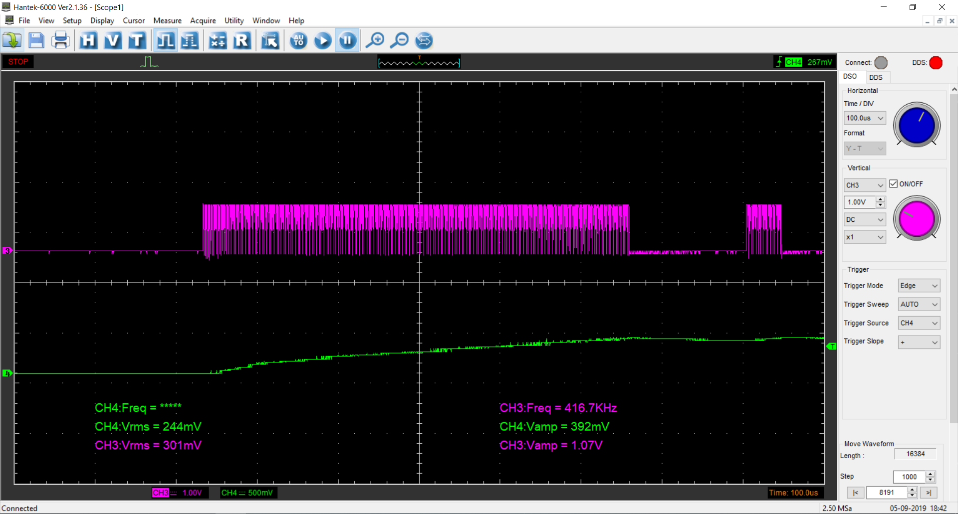
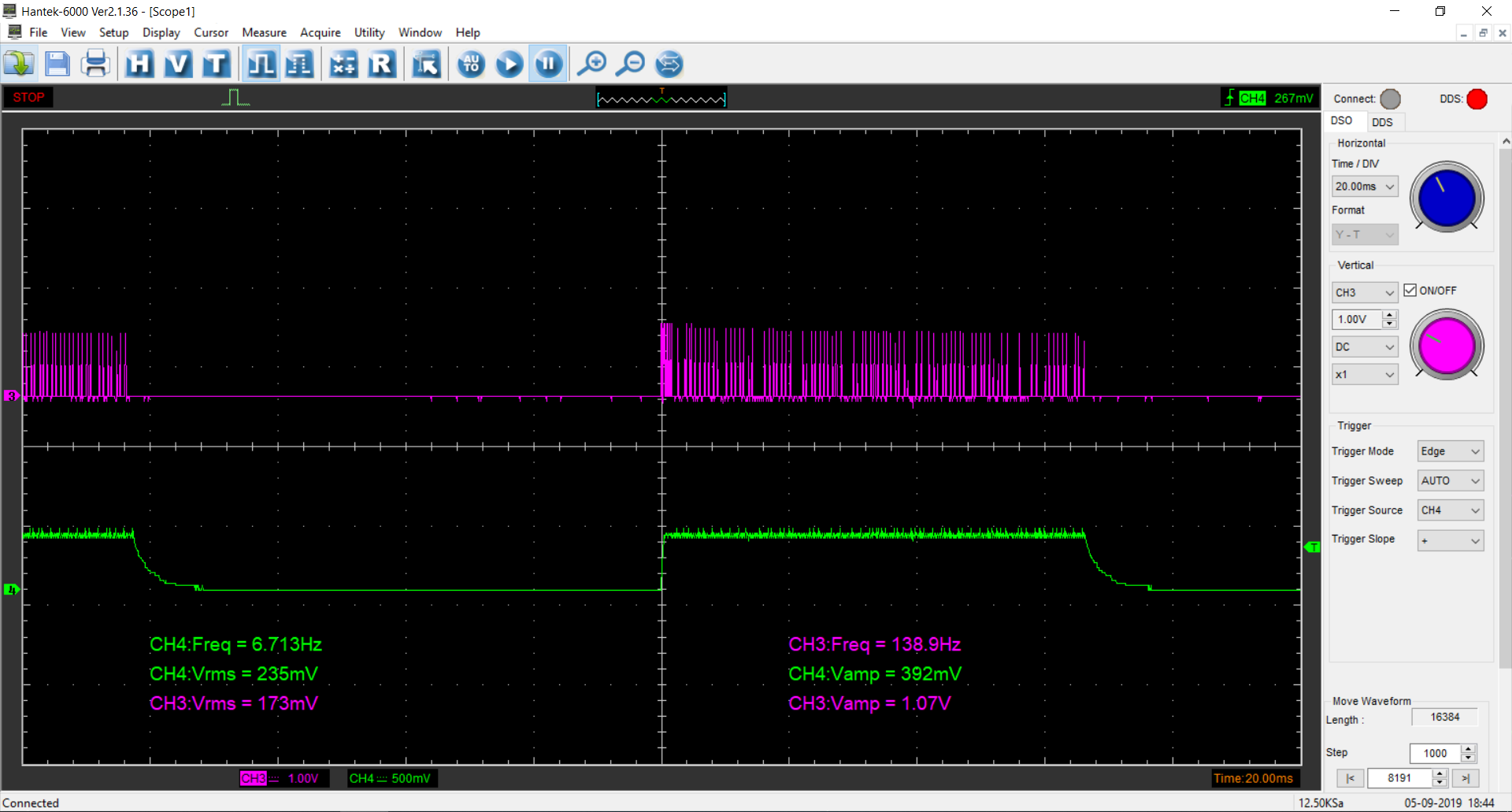
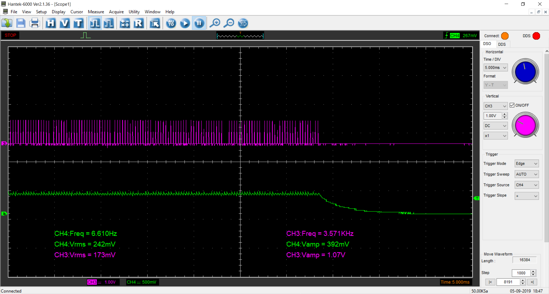
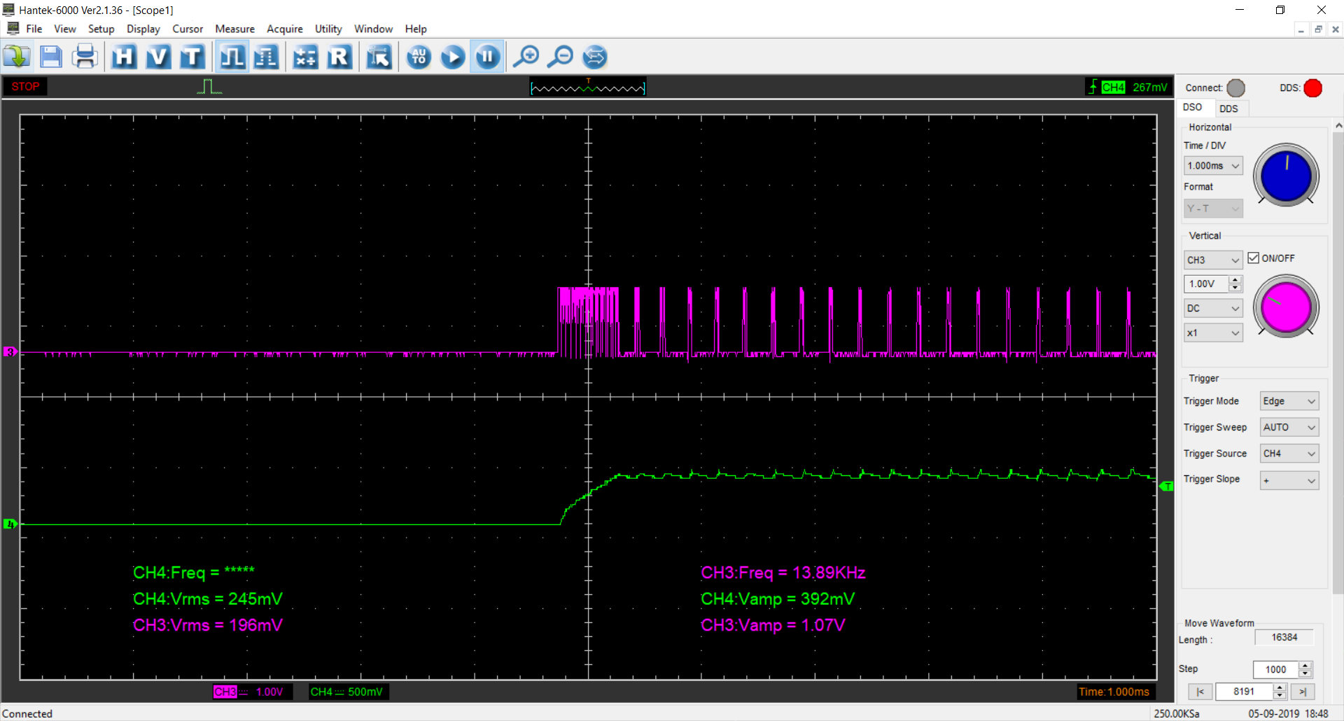
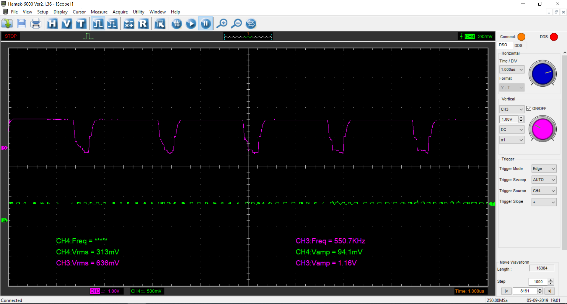
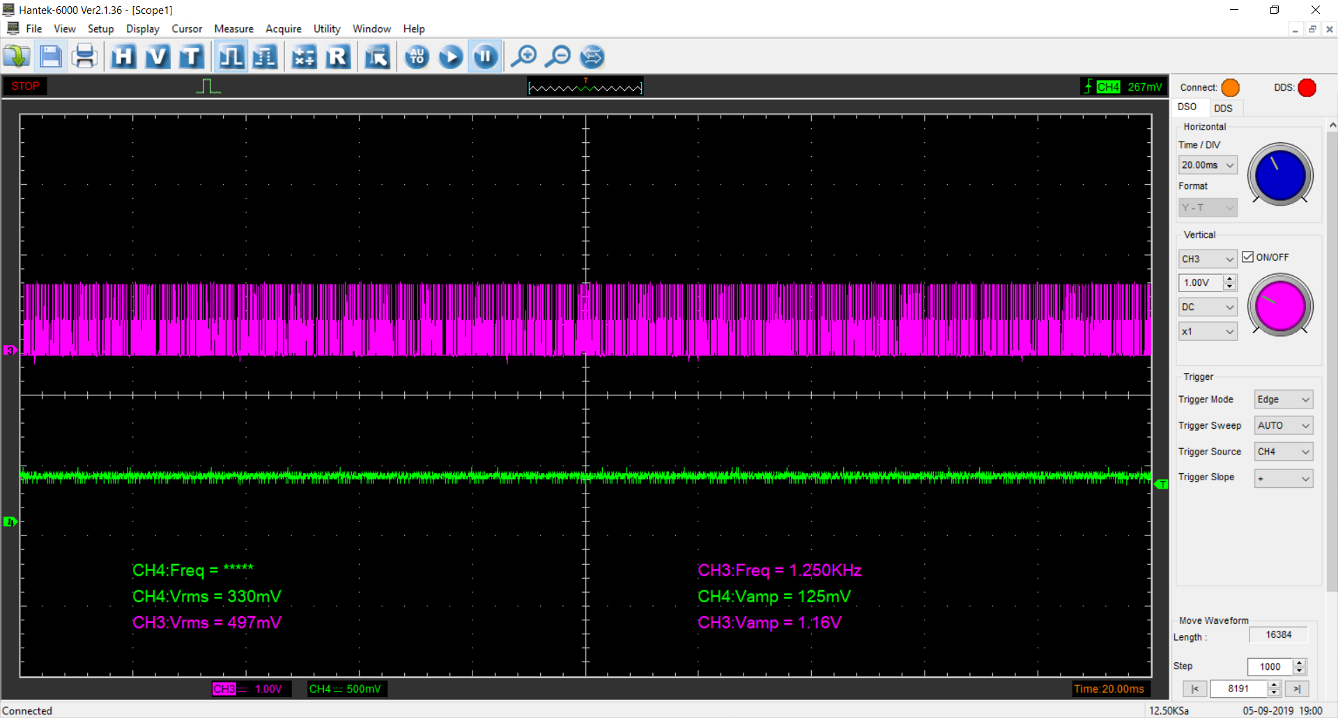
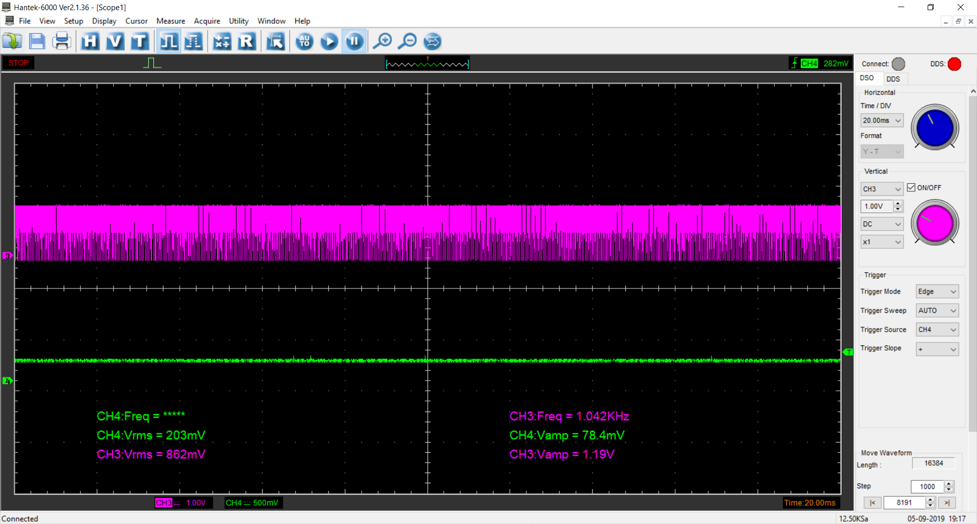
We are students and we try to design isolated dc-dc converter for our PLC project. We use UCC28C43D driver. Our project was designed by WeBench Power Designer (link to design webench.ti.com/.../6). When we tried to start up DC-DC feedback didn't work. We analysed device behaviour and found one problem. Resistor R12 had very small value and internal power supply was overload. We changed R12 to 1 kOhm resistor and voltage feedback was ok. But DC-DC behaviour wasn't ok. DC-DC had discontinuous operation. What could be the reason?

  • Hi Anton,

    Thanks for contacting us. Could you please share your Webench design? Please follow below steps.

    1. Create the Webench design and click on "Export" tab. Look for share icon just below it. Pleas click on it.

    2. Click "GET LINK" from Public Link tab.

    3. Share the generated link with us.

    Thanks and Regards,

    Umayal

  • https://webench.ti.com/appinfo/webench/scripts/SDP.cgi?ID=AD2C44BCEF190B14

    This is actual link to the last design.

  • Hi Anton,

    Can you share the Vds and Vout waveforms if possible? 

    Thanks
    sahil

  •       drain to source wave forms. Load 100 Ohm.

  • Hi Anton,

    Can you see if this behavior is observed when you increase the load to 50 ohms/10ohms/5ohms/1.65 ohms?

    We are checking on the compensation, meanwhile you can try to see if you are able to find the cause.

    Thanks
    sahil

  • I answer instead of Anton. As the output current increases, the pulse on the mosfet becomes more stable, and the output voltage decreases. What is the reason? Oscillogram for a slice.


  • on 5 Omhs


    on 1.6 Omhs

  • Hi Anton, Mikhail, 

    Thanks, 

    Can you confirm these things:

    a. Shunt regulator used in the board(it should be low voltage 1.24 Volts, LMV431). 2.5 Vref shunt regulator should not work for this low Vout?
    b. Current sense resistor value
    c. Voltage on COMP pin and voltage across R12 resistor(at Vinmin of 10 volts)
    d. Duty cycle value at Vinmin(10 volts) and Vinmax(28 volts)
    e. if you can share few details on transformer used for the design,that might help as well


    thanks
    sahil

  • Hi, Sahil. Result of measure on Comp pin and R12 in archive. R sense value 0.1 Omh, i tryed to use 0.3 omh, but changing the Rsense value does not change output waveform. About transformer: We use planar transformer based on N49 ferrite ELP 14/3.5/5. Number of coil on primary vinding 30, Calculating inductanse 533uH.Measure.rar

  • ok Mikhail, can you confirm the shunt regulator you have used , it should be low voltage 1.24 volts, ex: LMV431. 

    Thanks

    sahil

  • Hi Sahil! Today i checked shunt regulator. He opened at 1.24V

  • Hi Mikhail, 

    I will recommend to check the power stage by disconnecting the feedback loop. Remove the opto and sweep the voltage starting from 5 volts down to zero volts on R12 resistor on the board. This will help the converter start slowly to full load. During this, try measuring primary current waveforms, duty cycle, output voltage, etc to see if our power stage is well or not. 

    sahil

  • Hi Mikhail, 

    Did you get a chance to check the power stage as recommended by Sahil in above comment?

    Best Regards,

    Bhushan

  • Hi Sahil. Im sorry for long answer. I disconnected fellback as you recommended. When the voltage on the resistor is 0 volts the system operates in maximum fill mode.

     After about a couple of seconds, the outages begin

    Channel 3 - Voltage on primary side (mosfet Gate) CH4 output voltage.

    On another voltage - simular situation. On 2.6V on first second:

    and two second later:

    When voltage on R12 become more 2.7V module turn off.

    Once in the measurement received the waveform as in the picture, but this result at the same values more could not be obtained.

  • Hi Mikhail,

    I will recommend to take all the measurements on frequency scale,

    time/DIV of 1 uS should be ok. 

    Also we would want the primary side(MOSFET Drain to Source) voltage, secondary side voltage( across transformer sec winding) and Vout - waveforms on time/DIV of 1uS, along with measured values(waveforms+values). Right now, it might be difficult to assume the value of Vout from only the waveform above(green) .

    Also there is a possibility if we operated the converter at full duty cycle by applying voltage of 0 volts to R12 resistor, instead of starting from 5 volts on R12 and then slowly reducing it. So here.I will suggest start applying 5 volts on R12- then measure the output voltage, pri side voltage( drain-to-source), sec side voltage( even primary currents if possible). After this, keep reducing the voltage on R12, and observe Vout, pri voltage, sec voltage behavior. Keep reducing the R12 voltage till the point Vout settles to 3.3 Volt, and then stop at that R12 voltage level. This testing will give us an idea of whether Vout is starting from 0 volts and settling to final 3.3 volts by applying decreasing voltage on R12, and hence we can see whether the current designed power stage is working fine as expected. 

    However before doing this, i will suggest to verify whether the output diode and output capacitors are not damaged, from our previous testing, and then replace them if found.

    Once we verify the power stage first, then  we can go with loop testing. 

    Meanwhile, do we have the secondary turns and auxiliary turns of the transformer? - for pri- it looks you have 30 T from our prev replies. 

    Thanks

    sahil

  • Hi Sahil. What do you mean? "I will recommend to take all the measurements on frequency scale"


    Output diode and capacitor working in normal mode. I change voltage on R12 from 5 volts down to 0 volts. Beginning 2.68 volts i get impulses, but when i change voltage on feelback output voltage isnt change. In archive screenshots from oscilloscope to proof it. Channel 4 is output voltage, Channel 3 is drain to sourse voltage dropmeasurement2.rar. Channel 2 - voltage on secondary coil 3.3V

    About transformer. You totally right. Transformer have 5 secondary whire on 24, 7 to supply controller microscheme, 3.3 and two separate 5 output voltages. But feelback loop using one 3.3V coil. Other coils use linear stabilisator to set output voltage value. 

  • Hi Sahil! Thanks you for help. I found problem why my supply module unstability work. Supply for microscheme is so low, for this reason he always drop down. I corrected supply voltage, then microscheme get work stable. But i found new problem: feelback loop is not working. When i turn on the scheme on 50 omhs load on 3.3V coil input power become equal 75 Watt (15V 0.5A).

    When i Increase load resistance to 100 omhs, on R12 droop 2.5V, but output voltage dont go down

    Channel 2 - Voltage on r12 , ch3-output waveform, ch4 waveform on mosfet gate

  • Hi Sahil. I think, problem in transformer construction. How i can check scheme without transformer? I Remove mosphet from board and disconnected feedback loop. Then i appply voltage on R12. On picture maximum and minimum duty cycle which I got. Is this the correct mode of operation?


  • Hi Mikhail, 

    No problem, 7.5 W(15 V, 0.5 A) is pretty high and it should be getting dissipated somewhere in the circuit, due to some fault. There should be some component in the board getting heated. I will recommend running the power supply for some time, then shut it down and then touch each component on the board quick to see where the issue might be. 

    Thanks, 

    sahil

  • Hi Mikhail, 

    The duty cycle should not change if we remove the FET  as it would need the MOSFET and the current sense resistor along with transformer circuit, to compare voltage on COMP pin with the CS signal. 

    Right now the above change which we are seeing in above waveforms in duty cycle( 81 percent vs 71 percent) might be due to some noise. 

    So if we want to test out the whole scheme, we will need the transformer/FET/current sense. 

    If the transformer construction is at fault, then we might have to fix that first, after that we can check the power stage with the PWM controller. 

    Let me know if you think a call can help on this one, we can have one set up according to the time zone you are in. 

    If we only want to see whether the PWM controller is able to give varying duty cycle without power stage, that can be done by disconnecting FET and adding RC circuit to OUT pin along with a schottky diode. Then apply voltage on R12 as we did earlier. However this will only tell us whether the PWM is working fine. 

    For the whole scheme to test, we will need transformer/FET and other power stage components. 

    Thanks

    sahil

  • Hi Mikhail, 

    Did you get a chance to identify the power stage component getting heated on board as recommended by Sahil in previous post?

    Thanks and Regards,

    Umayal

  • Hi Sahil. Thanks for you answer. I staried scheme with another operable transformer, but operatidg mode doesnt changed.

    Channel 4 - on mosfet gate. With no load on secondary side. Ch 3 Voltage on R12. What the reason this operable mode?

  • Hi, Mikhail,

      The MOSFET gate pulse is determined by the COMP pin voltage and the current sense pin voltage.

      Looking at the block diagram, the MOSFET is turned off once the CS pin voltage reaches the processed COMP pin voltage (roughly COMP pin voltage minus 1.4V, and then divided by 3).

      In this case, you get getting maximum duty cycle. You need to figure out if the COMP pin is at its maximum value or your CS pin couldn't get enough voltage at desired duty cycle (basically, can't get enough current). Please help to measure the voltage on COMP  and CS pin so that you can see if the duty cycle makes sense.

      Once the CS pin voltage is measured. It can also tell you if the power stage is correct. Because CS pin voltage is essentially the primary side current multiplied by the current sensing resistor. You should be able to tell your primary side current, the primary side inductance.

      Let us know what you find out and we can help out more.

      Good luck.

    Bing

  • Hi Mikhail,

    Did you get a chance to measure voltage on COMP and CS pin as suggested by Bing in above post ?

    Thanks & Regards,

    Harish

  • hi. Thanks for you answer. I measuring voltage value on 4 channels: ch 1 - gate, ch 2 - FB pin, ch3 -  CS pin and ch4 - COMP pin.

    current consumption has become stable (70 ma), fellback loop working normal, but pulse width not changing (output voltage > 3.3V),and also there are interruptions in work. What the reason?

  • Hi Mikhail,

    There are some things we see in these waveforms:
    a. Gate voltage is going below zero. Even the gate pk voltage is distorted.
    b. The gate is skipping pulses even though CS signal is present. Maybe the CS signal is coming only from slope compensation ckt to CS pin and not from Rsns resistor, so in that case FET might not be switching at all.


    Based on these, we will recommend to check out these things.

    1. Measure the voltage on OUT pin of the IC - use channel 1. Keep the same scale as you did in previous snapshot for the channel 1.
    2. Measure the voltage on the Gate of M1 FET - use channel 2. Keep the same scale as you did in previous snapshot for the channel 1.
    3. Measure the voltage on Rsns resistor - use channel 3.( if you can measure transformer primary current if that is easy for you instead of voltage on Rsns resistor, that should also be ok)

    Store all these waveforms - "Waveform set 1"

    After taking these measurements, do the following steps.

    1. Measure the voltage on Drain of the M1 FET- use channel 1. Keep the same scale as you did in previous snapshot for the channel 1.
    2. Measure the voltage on the Gate of M1 FET - use channel 2. Keep the same scale as you did in previous snapshot for the channel 1.
    3. Measure the voltage on Rsns resistor - use channel 3. ( if you can measure transformer primary current if that is easy for you instead of voltage on Rsns resistor, that should also be ok)

    Store all these waveforms - "Waveform set 2"

    After doing this, add any schottky diode from OUT pin to Ground( cathode connected to OUT and anode connected to ground)

    Repeat these steps again:

    1. Measure the voltage on OUT pin of the IC - use channel 1. Keep the same scale as you did in previous snapshot for the channel 1.
    2. Measure the voltage on the Gate of M1 FET - use channel 2. Keep the same scale as you did in previous snapshot for the channel 1.
    3. Measure the voltage on Rsns resistor - use channel 3.

    Store all these waveforms - "Waveform set 3"

    1. Measure the voltage on Drain of the M1 FET- use channel 1. Keep the same scale as you did in previous snapshot for the channel 1.
    2. Measure the voltage on the Gate of M1 FET - use channel 2. Keep the same scale as you did in previous snapshot for the channel 1.
    3. Measure the voltage on Rsns resistor - use channel 3.( if you can measure transformer primary current if that is easy for you instead of voltage on Rsns resistor, that should also be ok)


    Store all these waveforms - "Waveform set 4"

    Let us know all these waveforms( set 1 to set 4), and then we will check the behavior.

    I am attaching a short snapshot here, in case any confusion for measuring waveforms at test points/placement of schottky diode, during checking out above steps. Let me know if anything. 

    measuring signals.pptx

    Thanks
    sahil

  • Hi, Sahil. I measuring as you say. 

    Waveform 1 (Whithout diode)

    Waveform 2 (Without diode)

    Waveform 3

    Waveform 4

    But i placed diode between mosfet gate and sourse. Placing him before Rdrv not changed output waveform

  • Hi Mikhail, 
    Thanks for the waveforms, 
    From what we see voltage across Rsns resistor is zero when gate is high, although it should resemble primary current waveform(~ triangular).

    That means either current sense resistor is "short" or there is no transformer primary current flowing in the circuit.

    Can you check these 2 things:


    a. Measure transformer primary current(between points A. and B. , from the attached snapshot)
    b. Check if current sense resistor Rsns is working properly( not shorted, etc)

    sahil

  • Hi Sahil. Thanks for you support. I found mistake in my scheme. It was the value on the cs resistor. I installed a low-rated resistor (0.01 Omh), but i thought he nominal is 0.1 Omh. Now i installed 10 Omh cs resistor and scheme started work.