This thread has been locked.

If you have a related question, please click the "Ask a related question" button in the top right corner. The newly created question will be automatically linked to this question.

LM5122: Unexpected voltage drop in output (hiccup overload?!)

Part Number: LM5122

Hello everyone,

I have a problem with a boost converter based on the 2PH EVM and hope somebody could help me find the cause.

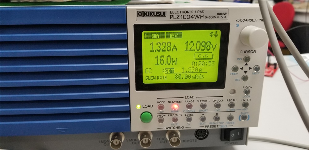
The converter works properly up to about ~1A   at 24V. When I go over that current, I will hear a noise and suddenly voltage drops to about10 to15V. It also happened in lower currents as well. It seems to be very random!

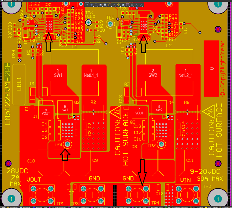
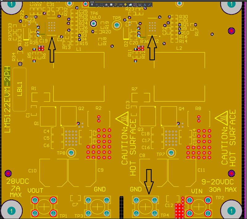
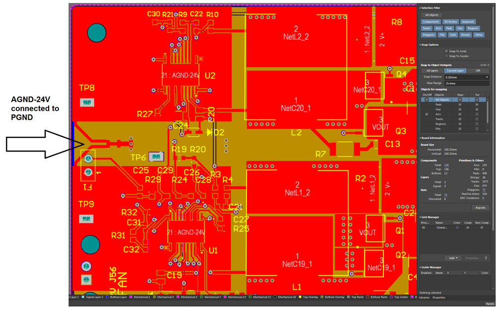
I read the forum and notice that it is mentioned PGND ANDAGND should be separated. In my 4layer PCB, they are not separated as it was not mentioned in schematic (see attached picture).

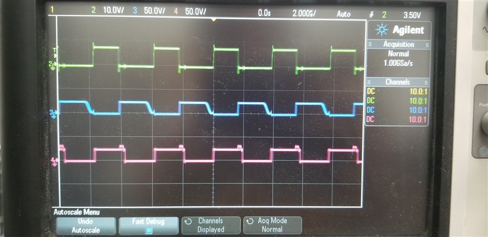
My layout has been made based on the LM5122EVM-2PH. I have checked my gate signals and they are clean as crystal! I don't know where the problem can be!? any idea?

  • Hello Babak,

    Thank you for reaching out with your questions.

    Can you please post the schematic and provide the application information? This will help us to fix the issue.

    Thanks,

    Garrett

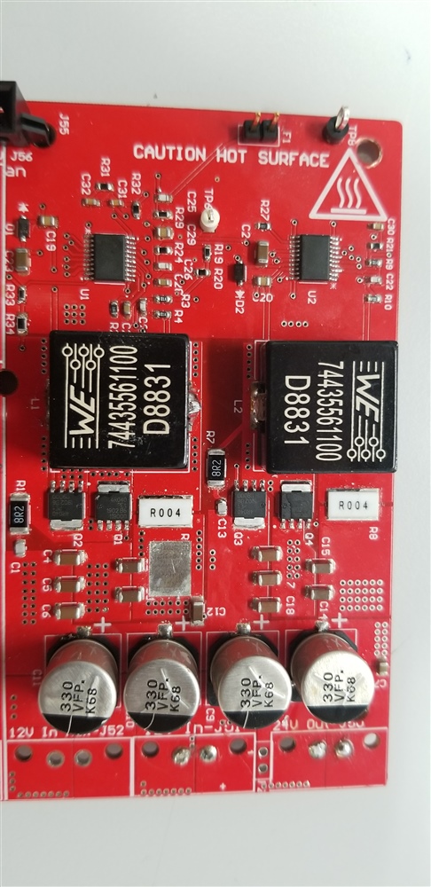
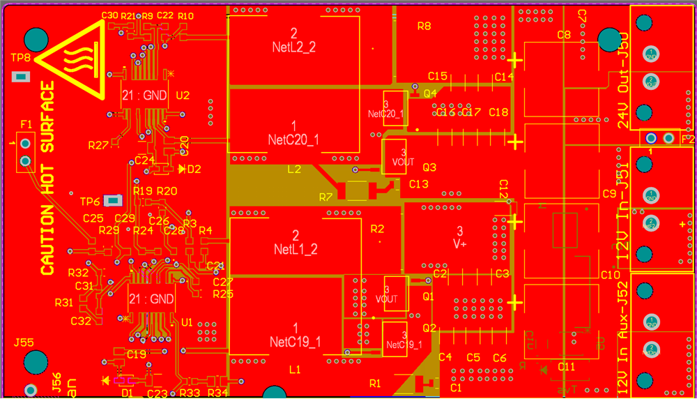
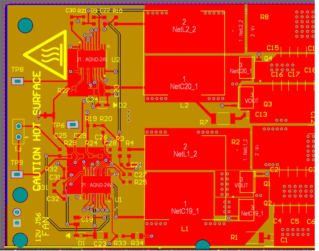
  • Here are the pictures of PCB and its layout. The schematic is exactly as 2PH EVM:

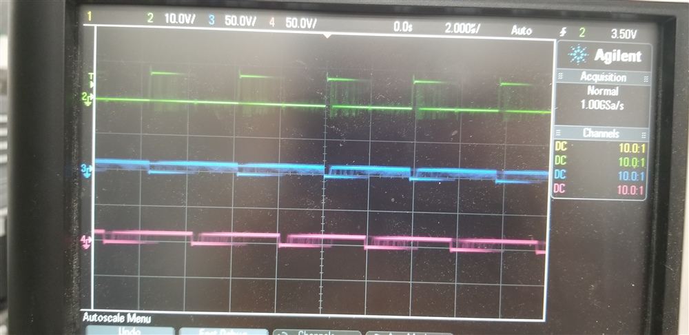
    Here is a picture of gate signals on normal operation:

    After increasing the load a little bit:

    Thanks,

  • Thanks for your reply Garret. Right now, I am just testing my PCB. I will use it for running 2 servos in the future. As I mentioned in my comment, Schematic is as same as 2PH EVM; however, I don't have a separate AGND and PGND in my circuit as it was not mentioned in schematics!?!

  • Hi Babak,

    Based on the waveforms provided it looks like this is probably noise related. The AGND and the PGND should be separate and then connect at the back of the LM5122. There will be an AGND plan for each IC.

    Another suggestion is to run the SW and HO trace as close as possilbe and then have the SW pin trace connect to the source of the high side MOSFET. This will help reduce the noise coupled into the gate drive loop and help stabilize the operation.

    Please also ensure that the current sense signals are routed away from the switch node and the traces are close together.

    Let me know if you have any questions.

    Thanks,

    Garrett

  • Thanks Garrett for your reply. I also think it is a noise related issue. I wish you guys could modify the datasheet so people know they need to separate PGND and AGND.

    A separate  AGND for each IC was also something that I didn't think about.

    Regarding the current sensing signal, as you can see in my PCB layout; they are way far from switches. DO you think I still need to move them?! I can send you my PCB design to have a look.

    Also, Can I ask for Altium file of your design so I can check to see if there is anything else missing in my design?

    Thanks,

    Babak

  • Hi Babak,

    Regarding the current sense I cannot see the current sense traces. I am assuming that these are an internal layer. If these signals are shielded from the SW using a ground layer then then the signal should be good. I also recommend making the COMP signal shielded from the SW node as well and make the traces a short as possible. Please see the attached Altium project for the 2 phase LM5122 EVM.

    SV600881A_Source.zip.

    Thanks,

    Garrett

  • Hey Garrett, Thank you for the link. I had a look at your file and have a question for you.

    I notice there is no PGND in your PCB design! In Top Layer, SGND for each IC is separated from each other and also from input ground (it is called SGND again!), but in the next layers (MIDLayer1&2 and bottom), they are all connected to each other! 

    When you mentioned that PGND should be separated from AGND, my assumption was that they need to be separated everywhere and the get connected by a small pad. Is that right?

    Cheers,

    Babak

  • Hello Babak,

    The AGND polygon (SGND in this design just a different name) is on the top layer it is connected to the AGND pin that is then connected to the exposed pad of the LM5122. The exposed pad is then connected to the ground layer (PGND and PGND pin) and then connected to the second layer which is the boards ground layer. This creates a star connection of the grounds right under the LM5122 which helps mitigate noise on the IC. AGND and PGND need to be tied together to ensure that the planes are at the same potential.

    Thanks,

    Garrett

  • Hello again Garrett,

    I have redesigned my PCB and separated the two IC grounds and then connected to the exposed pad. The exposed pad is also connected to PGND using three vias. Do you think this configuration works? I appreciate your idea on this.

    Thanks,

    Babak

  • Hello Garret, I modified the circuit a little more and now looks like the TI circuit. Please comment on this one. Thanks

  • Hi Babak

    It looks pretty good. I suggest to also add VIAS on the exposed PAD of the LM5122 and tie these to the ground layer. This will help to keep the LM5122 cool.

    Thanks,

    Garrett