This thread has been locked.

If you have a related question, please click the "Ask a related question" button in the top right corner. The newly created question will be automatically linked to this question.

Charger ic selection

Other Parts Discussed in Thread: BQ24103A, BQ25606

Hi,
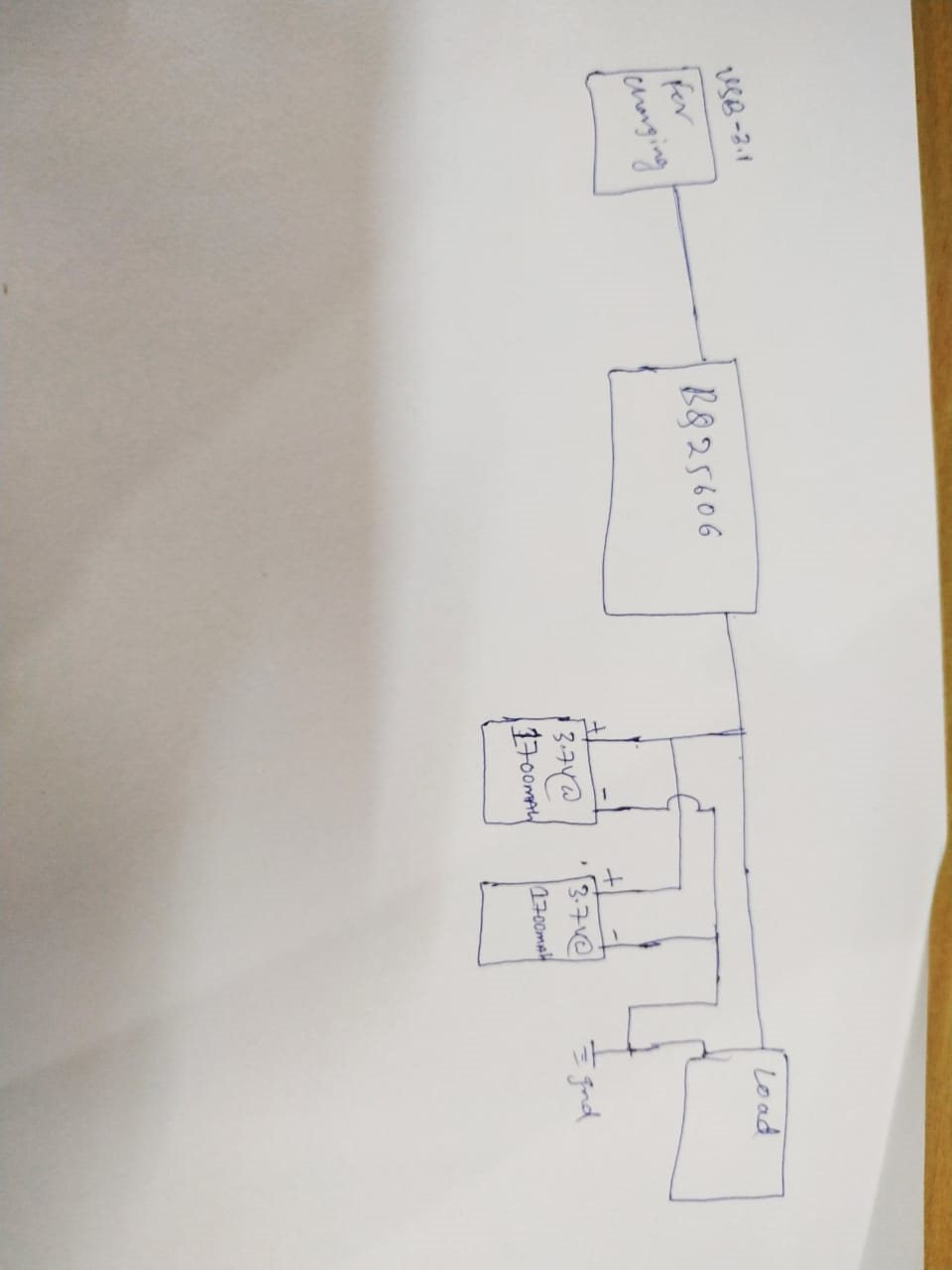
We are using two lithium polymer battery in parallel combination each one has a capacity of 3.7V @ 1700mAh.
And we are planing to use bq24103A IC from ti.is it ok to use please confirm.

and also we are charging from USB.

or suggest me any better ics from ti.

Thanks,

Ashok

  • Ashok,

    Parallel Li-Ion batteries self balance.  BQ24103A will be okay to use for charging although charging a 3400mAh battery with only 2-A will require close to 2 hours for full charge.  If your USB source can provide 5-V, 3-A, you might consider changing to BQ25606 3-A, all integrated charger.

    Regards,

    Jeff 

  • Hi Jeff,

    Thanks for the support.

    Can i use BQ25606 for 3A charging.

    Thanks,

    Ashok

  • Hi Jeff,

    Thanks for the support.

    Can i use BQ25606 for 3A charging. and  we  are connecting two parallel 3.7V@1700mAh Batteries for this configuration is it ok to use BQ25606  iC.

    Please confirm. below attached our block diagram.  

    Thanks,

  • Ashok,

    Your block diagram should work.

    Regards,

    Jeff

  • Hi Jeff,

    Thanks for your continuous support ,

    Can i get BQ25606 schematics,BOM,PCB layout.

    Thanks,

    Ashok 

  • Ashok,

    Please see attached.

    Regards,PWR772B (9-23-2019 7-37-08 PM).zip

    Jeff

  • Hi Jeff,

    Thanks for the design file.

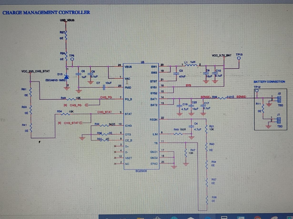
    Below attached our 3A charging design schematics and usb schematics.

    Can u please confirm the schematics and give me feedback if any addition need to be done.

    And also one conformation from your side is,

    What is the maximum output current of SYS without battery when the adapter is connected to VBUS.

    Thanks,

    Ashok3010.SCHEMATIC1 _ PAGE1.pdf

  • Hi Ashok,

    C30 is 4.7uF not 4.7nF.  Other than that, I see no obvious schematic errors.

    Regards,

    Jeff

  • Hi Jeff,

    Thanks for your time.

    Can i know 

    What is the maximum output current of SYS without battery when the adapter is connected to VBUS.

    Thanks,

    AShok

  • Ashok

    Per datasheet section 7.3 Recommended Operating Conditions, the max ISYSOUT = 3A.  This will be split between ISYS and IBAT with ISYS taking priority.

    Regards,

    Jeff

  • Hi Jeff,

    Thanks for you time and continuous support,

    We designed  BQ25606  circuit on single layer board.

    Is it ok  to use Please confirm.

    does it affect on any performance issue ? 

    Thanks,

    Ashok

  • Hey Ashok,

    At a minimum for this device, you will need a 2 layer board. The second layer will be needed for a proper ground return.

    Regards,

    Joel H

  • Hi Jeff,

    Thanks for your support .We are testing charging ic. Battery is not charging.

    Below are test reports.

    Input voltage-5V

    Power good-low

    STAT Pin - High

    battery voltage 3.5V Capacity 2000mAh.

    Ntc We are not using so i connected 10K And 10K Ohm.

    And also input voltage and current is 5V And current fluctuating from 0.1A to 5mA.

    Below attached out schematics for you reference.

    Thanks,

    Ashok


  • Hey Ahok,

    We recommend at least 20uF of capacitance on SYS. You only have 10.1uF.

    Be sure that the /CE pin is truly low, and that the BAT pin voltage is below the 4.2V regulation voltage.

    Regards,

    Joel H

  • Hi joel,

    Thanks for your time.

    We changed capacitor value to 22uF.

    Below are the test reports without battery:

    Input supply voltage : 5V @ 36mA Without battery connection.

    Bat vin voltage without battery 3.3V to 4.2V Fluctuating.

    Sys pin voltage without battery 3.3V To 4.2V Fluctuating.

    Vset pin open

    STAT Pin :  blinking

    PG Pin : low

    CE Pin : low 

    Below are the test reports with battery:

    Input supply voltage : 5V @ 130mA With battery connection.

    Bat vin voltage with battery 3.5V Battery voltage .

    Sys pin voltage with battery 3.5V Battery voltage .

    Vset pin open

    STAT Pin :  1 Min Low after 1 min 2.1V To 2.5V

    PG Pin : low

    CE Pin : low

    And also after 2 min input supply current  Fluctuating from 0.135mA to 80mA.

    finally battery not charging.

    Please let me know if any changes need to be done in schematics.

    Thanks,

    Ashok

  • Hey Ashok,

    Two things:

    1) For your test without a battery, the behavior is normal. Because there is no battery present and charging is enabled, the output voltage climbs up to the charging regulation voltage and drops again when charging is terminated.

    2) For the second condition with a battery, it sounds like you may have a large impedance between the battery and the BAT pin of the charger. When the charger enters the termination threshold, the battery voltage tends to relax. If the battery voltage (as seen at the BAT pin of the charger), falls below the recharge threshold due to the high trace/line impedance + significant battery relaxation, you could see this behavior.

    Regards,

    Joel H

  • Hi Joel H,

    Thanks for the suggestion.

    we designed new two boards 1) one in single layer.

                                                    2) other one in two layer

    1) Below are the test results of one layer board 

    input voltage : 5V current support upto 5A

    STAT Pin : High.

    PG Pin : low 

    Vset : open 

    CE Pin : gnd.

    OTG Pin : Gnd.

    Bat pin : Battery voltage 3.5V

    Sys pin voltage : 3.6V.

    No Load on sys pin 

    Input current fluctuating form 3mA to 15mA. 

    Finally battery not charging.Below attached schematics and layout of both single and two layer layout file  please check and confirm.

    2) Below are the test results of two layer board 

    input voltage : 5V current support upto 5A

    STAT Pin : low.

    PG Pin : low 

    Vset : open 

    CE Pin : gnd.

    OTG Pin : Gnd.

    Bat pin : Battery voltage 3.5V

    Sys pin voltage : 3.6V

    No Load on sys pin.

    battery charging at 1.2A not 2A . we design i charge of 2A ie Rlim is 340 ohm  . 

    why its working like this.Please suggest me if i missed out anything in design.

    Our customer looking for single layer board solution.is it ok design BQ25606 in single layer please confirm. 

    pdf_CHARGER_IC_DESIGN.pdfCHARGER_IC_DESIGN.brd

  • Hi Joel,

    Any suggestion.

    Can i get your mail id.

    Thanks,

    Ashok

  • Hey Ashok,

    I looked at your layout and the ground loop is very poor. The impedance between PMID and the charger PGND plane must be very high as compared to the EVM. A very thin trace around the inductor is the only path to PGND. Similar things can be said for the BAT net and any other trace sitting on the BAT net.

    I don't believe the critical filtering capacitors are making a filtering loop back to the IC ground.

    I would also make sure that the thermal pad is connected to the ground plane.

    If you refer to the Layout Guidelines in the BQ25606 datasheet, you will note the critical capacitors and traces, which in your board design may not be providing the required effect for both stability and regulation accuracy.

    Regards,

    Joel H

  • Hey Ashok,

    Any comment on the above? I just want to be clear that I still think your best option is a two layer board, at the very least.

    And the second layer must effectively be a solid ground pour. All non-ground pin can be routed on the top layer.

    Regards,

    Joel H

  • Hey Ashok,

    If your issue has been resolved, I will close this thread. Feel free to post a new thread if you have any further questions. 

    Regards,

    Joel H