This thread has been locked.

If you have a related question, please click the "Ask a related question" button in the top right corner. The newly created question will be automatically linked to this question.

LM5170EVM-BIDIR: Boost operation without LV-E-:oad and HV-PS

Part Number: LM5170EVM-BIDIR
Other Parts Discussed in Thread: LM5170, LM5170-Q1

Hi,

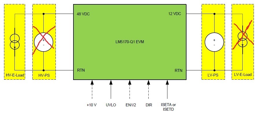
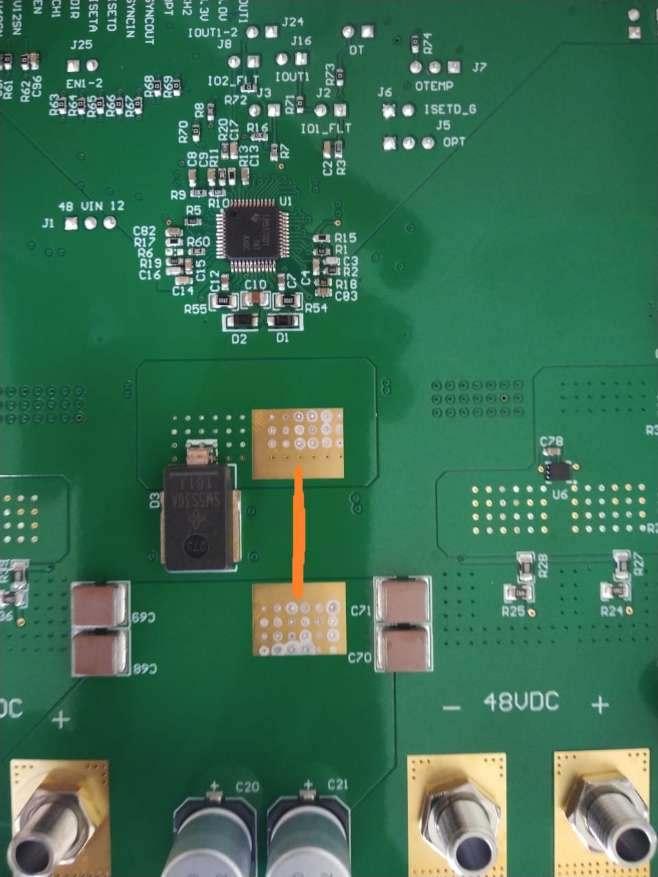
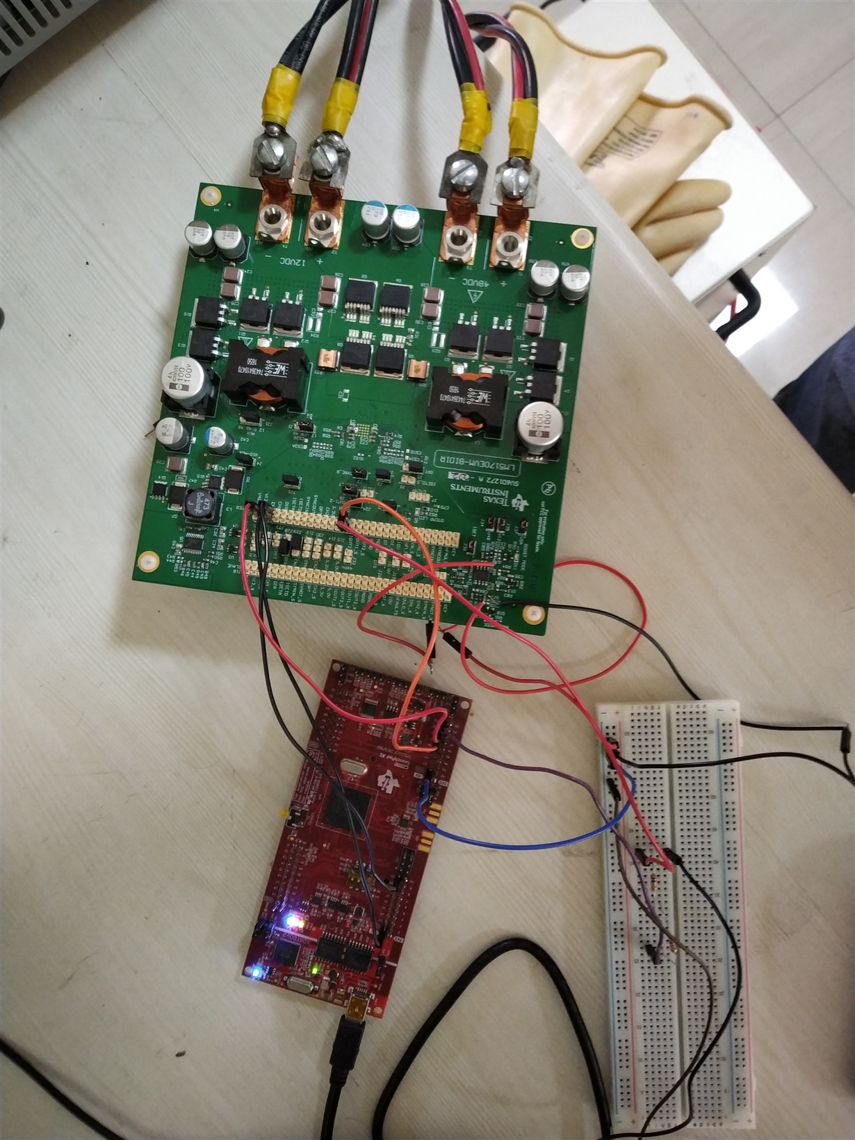
I am trying to test the EVM module for normal boost operation. In the test procedure, it is written that HV-PS is required for start-up in boost mode, if not MOSFET breaker should be shorted. How to short? I have seen another similar thread where copper foil must be used to short.

Whether I should solder as shown in the above image?

  • Hi Praveen,

    Thank you for your interests in the LM5170.  You are right, the two exposed pads are reserved for the shorting of the breaker FETs.   Please also do the following, to operate the EVM.

    1. Soldering 100k to R4 (factory default: not installed).

    2. Close J1 jumper to "12" side.

    3. Close J21 jumper to "12" side..

    4. Close the following jumpers: J2, J3, J4, J8, J34, J35, J36., J37

    5. Colse J5 to "OPT" side.

    6. Close J28 to "DIR" side

    7. Close J29 to "J29" side.

    8. Close J25 if you want to run dual phase.  Keep it open if you just want to run the 1st phase.

    9. To adjust boost output voltage, change R22.

    Good luck in your evaluation.

    Best Regards,

    Youhao Xi, Applications Engineering

  • Thank you. I have a few more doubts. For closing jumpers, 2.54mm jumper caps are suitable, right?

    1. Whether these changes interfere with the operation if I have to operate in normal buck mode?
    2. Other than changing R22, is it possible to maintain the boost voltage (suppose 48V) using external MCU (F28379D launchpad)? If so, how to do it? If any examples of coding or documents available, kindly share. Is it same as 9.1.4 in LM5170-Q1 datasheet? I will be using Simulink to interface my control algorithm.
    3. Basically LM5170 is known as a current source and can regulate the current. As per my understanding, it means I can control the output current (suppose normal boost. Battery at LV and load at HV) and it can be done using external MCUs too right?

  • Hi Praveen,

    You are welcome. Sorry I am not sure about your which type of jumper that you referred to.  Please use the same type as the ones delivered along with the EVM.  To your questions:

    1. The answer is no, except that you need to change DIR jumper to the other side to select boost mode.

    2. You still need to control the voltage feed back node, which is at R22.  When the launch pad produces the control signal (I guess in PWM), you need either to use an DAC, or a simple RC filter, to convert the digital to an analog signal, then feed the analog signal through a resistor to the R22 node.  By doing this, you can control the output voltage. 

    3. For buck mode, the answer is absolutely yes.  The LM5170 regulates the inductor dc current, which is the basically the load current.  For the boost, it is the input current.  You will need you MCU to do a calculation:  Iout = Iin x Vin/Vout.  Since the LM5170 can produce high efficiency, the calculation is close.  However, if you want precision load current accuracy for the boost, you will need to use external circuit to measure.  You can consider the INA devices from TI. 

    Thanks,

    Youhao  

  • Hi,

    Thank you. The information was very helpful. Would like to know further,

    1. Instead of changing jumper in DIR, Can I control boost or buck mode using an MCU? If I am not wrong, I read similar that in the datasheet. I want to change the boost and buck during operation. For example, the battery may discharge in boost mode and load can charge the battery in buck mode.
    2. Regarding voltage feedback at R22, I can see from the datasheet, it is connected to the gate of the MOSFET, I will try feeding the PWM through DAC and test it. Physically how to do it? Take a wire from R22 and apply PWM through DAC?
      Also is there any formula to calculate R22 for required boost voltage? I need 48V at the boost stage( at 48V PIN).
    3. With these changes hope I can move on to test the EVM for boost (24V to 48V) with a 10A or little more load. If anything else I should keep in mind, kindly let me know. Thank you very much.

  • Hi Praveen,

    1. Yes you can control DIR by an MCU. 

    2. Oops, not sure how I got that typo.  Its not R22 at all. 

    To adjust buck output voltage, you need to inject the DAC control signal to R78 via a feeding resistor.  For boost, you need to inject the DAC voltage to R77 via another feeding resistor. 

    You need to solve the resistor network:  R76, R78, and R_adj_buck, between the three voltages:  your desired buck Vout, DAC voltage, and the REF (2V here on the EVM), for the buck mode; and R75, R77, and R_adj_boost, between your desired boost output voltage, DAC voltage, and REF (2V here). 

    These are simple resistor networks, and you should be able to solve it.

    Good luck.

    Thanks,

    Youhao

  • Hi,

    I have found all the resistors mentioned except R_adj buck and R_adj_boost in the schematic. Kindly let me know the part number in the schematic.

  • Hi Praveen,

    These are extra, not on the EVM yet.  You need to build a small circuit, on which you put your DAC, and the output of the DAC needs to be connected to the said resistors via a resistor which is called R_adj.   You need two, one for buck and one for boost.

    Thanks,

    Youhao

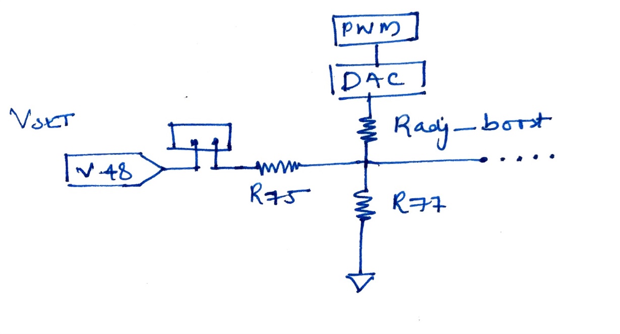
  • Okay, I was thinking R_adj and feeding resistors were different. As per my understanding, R_adjs are feeding resistors which must be connected to R78 & R77. Please correct me if am wrong, these resistors are just voltage dividers, right?. Also, I have attached a circuit diagram as per my understanding.

    In case I am wrong, please provide a rough circuit diagram. Thanks.

  • Hi Praveen,

    You are correct in your understanding. The DAC should be able to change the output voltage in this way. In your drawing please make sure that the jump is closed to ensure the circuit works properly.

    Thanks,

    Garrett

  • Can you elaborate on selection of that Res_adj with equation if possible? 

  • Hi,

    Sorry I am currently on a business trip.

    This is a simple resistor network.  First, you need to create a set of equations constraining these three resistors. 

    For your desired min output voltage Vo1,  your max control signal from the DAC and the desired output voltage Vo1 will produce a voltage at R77 that equals to Vref (2.0V on EVM).  So, this creates the first equation.  This links Radj and the max DAC voltage.   From which you can determine Radj.

    For your desired max output voltage Vo2, your second control signal from the DAC and desired output voltage Vo2 will also produce a voltage at R77 that equals to Vref.  Then you get the second equation relating Radj and the 2nd DAC voltage.  From it you can get the min DAC voltage.

    Thanks,

    Youhao

  • Hi,

    Still, there is some ambiguity in my understanding when you have mentioned "second control signal from DAC" .

    Well, as per my understanding I have solved the network for the following specifications.

    Incase of boost,

    Vo1,min = 46V

    Vo1,max = 48V

    Vdac_max = 3.3V

    R75 = 49.9kOhm

    R77 = 2.10kOhm

    I think something wrong in the equation below which I used to calculate.

    I have found out Radj_boost value to be approx 1.63k Ohm, but getting wrong min DAC voltage (Greater than Vdac_max used to calculate Radj). 

    I may be missing some simple points here, if not busy please provide the equation.

  • Hi, I would like to confirm some basics of the network in EVM for my understanding.

    1. The voltage across R77 i.e Vref, is it constant at 2.0V? If so, how my change in PWM affects the voltage due to Radj?
    2. My output from the control board (F28379D launchpad) is a pulse of 3.3V, whether I need a DAC in that case? Whether the output of DAC looks like a pulse?
    3. A scenario where input voltage (LV) changes and should maintain output voltage (boost)

      For example, my input at the LV side is a supercapacitor of 32 V and I have to maintain the HV side voltage at 48V. The supercapacitor voltage can go as low as 16V in our case. Hence, the duty ratio must be changed to maintain the 48V. In this configuration, do I need to make any other changes? 

    Overall, as I understood, these (R77-R75) are inputs of the error amplifier whose ref is 2V. But I am not able to understand, how connecting PWM through DAC at R77-R75 junction helps us in controlling the desired output voltage. How the voltage across R77 looks like when I use external PWM through DAC? Could you please clarify. 

    Thank you.

  • Please solve the following equations:

    (Vo1/R78 + Vdac1/Radj) /(1/R78 +1/R77 +1/Radj) = Vref,  where Vref=2.0V on the EVM.

    and

    (Vo2/R78 + Vdac2/Radj) /(1/R78 +1/R77 +1/Radj) = Vref,  

    You may solve by giving Vo1 and Vdac1 to get Radj from the 1st equation.

    Then, put Raj value into the 2nd equation.  Giving Vo2, you will get required Vdac2, which is required command to produce Vo2.

    Thanks,

    Youhao

  • Thank you very much. I think it should be R75 instead of R78 right?

  • Hi,

    What is the proper way to give a control signal at R77 resistor in the board?

    Since I never worked on SMD devices, it looks very small to solder any external wire to it. Kindly let me know the usual/professional way to give my DAC signals via Radj.


    Thanks.

  • You need to solder two wires, one on GND and one at the R77.  You should be able to solder a small wire to it. If not, you may need to get help from your technician able to do bench soldering.

    Thanks,

    Youhao

  • Hi,

    I have few more doubts on LM5170EVM. Kindly let me know the details.

    From the datasheet, I can see V48SN and V12SN for sensing the voltage during operation. Whats is the voltage range at these terminals and the gain factor? I couldn't find it in the datasheet.

    Also, J24 can be closed for a combined current monitor for ch1 and ch2. Where should I see this current, Pin27/Iout1? Also, what's the gain factor to calculate the actual current?

  • Hi,

    All these info can be found on the EVM schematic.  Please read the schematic.

    Specifically,  V48SN and V12SN are OVPA and OVPB respectively.  The gain is calculated by the OVPA and OVPB setting equations. Please refer to the datasheet.

    Regarding J24, once you close J24, you basically parallel IOUT1 and IOUT2, so, either Pin27/IOUT2 or Pin29/IOUT2 can read total current.  The gain factor will be doubled. 

    Thanks,

    Youhao

  • Hi,

    Similar to the above relationship, I was trying to solve at the LV side to regulate output voltage during buck.

    I need to regulate the LV side at 32V during buck. It looks like the onboard voltage loop control can be used to regulate to max 14.5V also OVP threshold is 22V

    I think the following changes can achieve what I am looking for,

    1. Recalculate Rovpb for VLV_max = 32V (Rovpb close to 38.45kOhm
    2. Recalculate R76, R78 to get Vref (= 2v) for VLVM_max (Calculated values: R76=22k and R78=1.5k)

    Whether the approach is correct? Is there anything else to change or any other method?

  • 1. You need to set your OVPA threshold to be higher than 32V, or you may hit OVP.  You need to leave at least 10% margin. I recommend to use 34.8k.

    2. for the EVM, I don't recommend to touch R76.  To adjust voltage setting, please just change R78, which should be about 1.78k. 

    Thanks,

    Youhao  

  • Thank you.

    How much current (max) will pass through the MOSFET breaker shorted wire? (shorted for normal boost operation)

    Regarding OVP, cant I apply above 22V supply at LV side during boost mode?

  • If  you solder a piece of copper file, you can easily pass the EVM rated current of 60A. 

    Yes you can, OVPB is ignored in boost mode.

  • Hi,

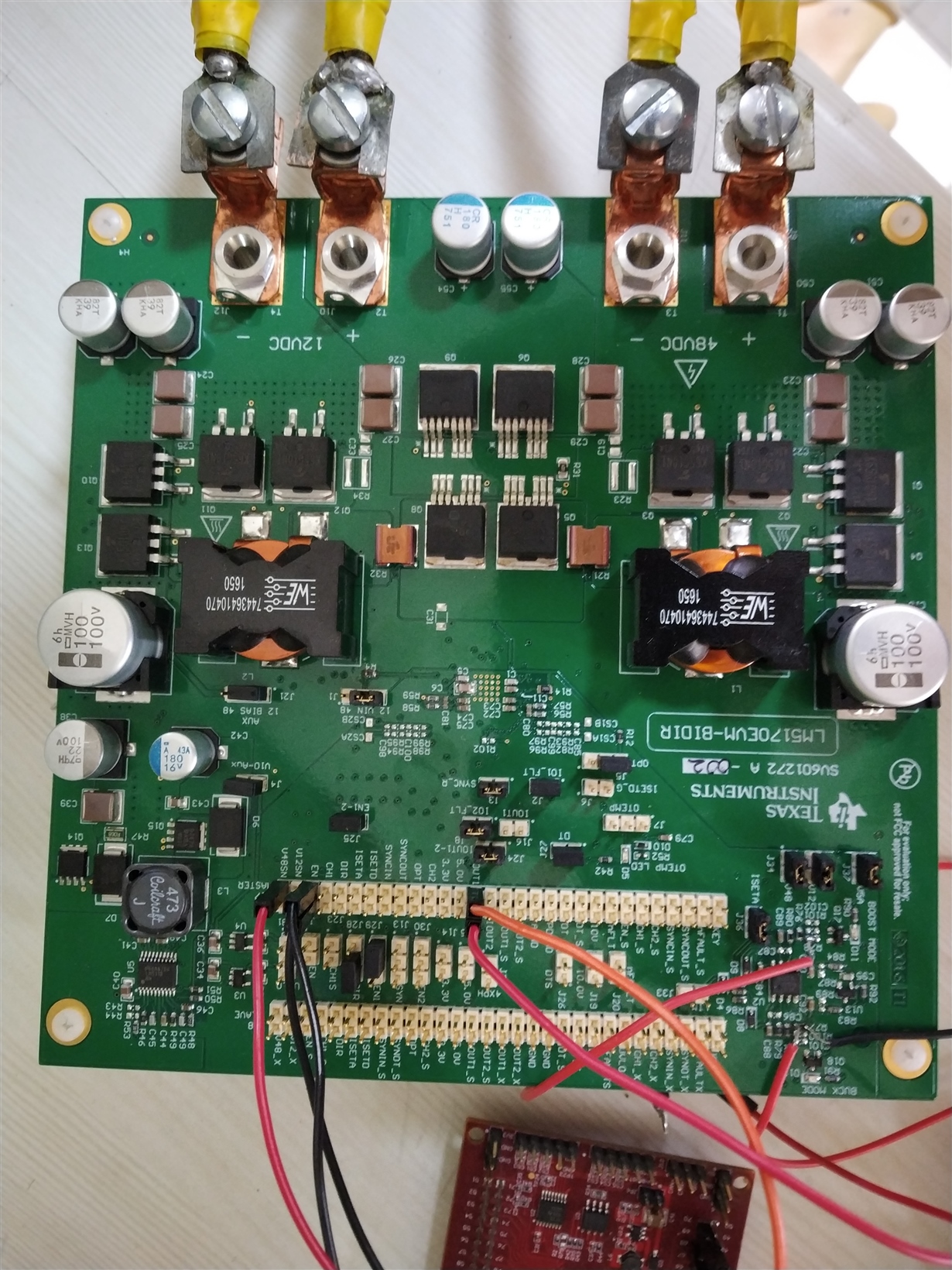
    From previous discussions, I have made all the required changes and tried to run the EVM in normal boost mode with a DC supply and a motor load. I have to maintain the output voltage at 48V as of now.

    DC Supply at LV side: 24 V and current limit 15A

    Motor: 48V,  no-load current: 6A (I didn't fully load the motor, running at no-load, so minimum current )

    1. I have made the necessary jumper changes as mentioned earlier
    2. Shorted the MOSFET breaker using a wire (20A current capacity) (copper file/foil is not available at this point)
    3. Connected small wires at R77 and R78 for regulating the output voltage, and at the ground.
    4. R4 100kOhm connected
    5. VDAC max is 3V and Radj is 14kOhm. 

    The output voltage at the HV side is the same as the input voltage (LV Side: 24V) during the boost operation. Also, the boost mode LED doesn't glow. 

    I am not able to find out the fault. Can you point out possible mistakes to debug?

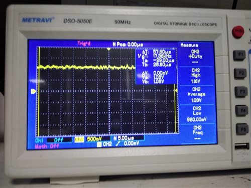
    Below image is the voltage at R77 node.

    Note: Instead of DAC and Radj, I have also tried directly giving Vref at R77 node.

  • If the light is not on, you may lose the +5V bias.  Check the +5V bias rail. 

  • Hi Praveen,

    Lets close this thread and open an new one.  This becomes too long...

    Please open a new post and lets continue discussion with it. 

    Thanks,

    Youhao