This thread has been locked.

If you have a related question, please click the "Ask a related question" button in the top right corner. The newly created question will be automatically linked to this question.

TPS63020: Seeking tips for reducing bounce on EN input

Part Number: TPS63020

I found an issue on this forum that seems to describe a problem we are having with the TPS63020 locking up in a shutdown state: .  We have a battery powered design that is recharged from a solar cell.  The output voltage from the TPS63020 is set for 3.35V and it includes a 0.5F supercap.  Some parts have a very wide operational voltage range (down to 1.8V), so to save power we disable the TPS63020 by default and only turn it on when needed.  In some cases we can run off the supercap for hours before re-enabling the TPS63020.  We have the EN pin tied high through a pullup resistor but then are using an NMOS transistor with a path to ground to disable the TPS63020.  We suspect that either the high switching speed or other power/ground plane transitions are causing the EN pin to bounce to a negative voltage and cause the lockup.  We haven't been able to measure to confirm; every time we attach a test probe to the EN pin everything works fine.

Assuming this is the case, do you have suggestions on how to reduce possible signal bounce on the EN input?  I don't want to post schematics or PCB layout in the forum posts, but I can private message someone from TI and share this information.

Thanks,

Bryan

  • Hi Bryan,

    I assume that the solution where you have the probe permanently attached to the EN pin is not acceptable :).

    If so, could you please send us the schematic and the PCB layout to:

    lbs_request@list.ti.com

    and I will look into it. You don't have to send us the complete schematic/layout, just a snippet of the area around the TPS63020 is enough, ideally showing the PCB layers in separate images. It is possible that the GND routing is not optimal, and attaching the probe ground makes it a bit better.

    Additionally:

    1. Can you please describe in more details the conditions and the sequence when and after the latch-up occurs. Does it occur during the rising or falling edge of the EN pin signal?
    2. Can you reproduce this issue while probing the signal that drives the NMOS, and if so, send us the scope plots of VIN, VOUT and the driving signal?

    Best regards,
    Milos

  • Milos,

    Yes, my boss didn't like the additional cost and size of an oscilloscope shipped with every device.  :)

    I'm compiling the email with additional information.  You should see it this afternoon.

    Thanks,

    Bryan

  • Milos,

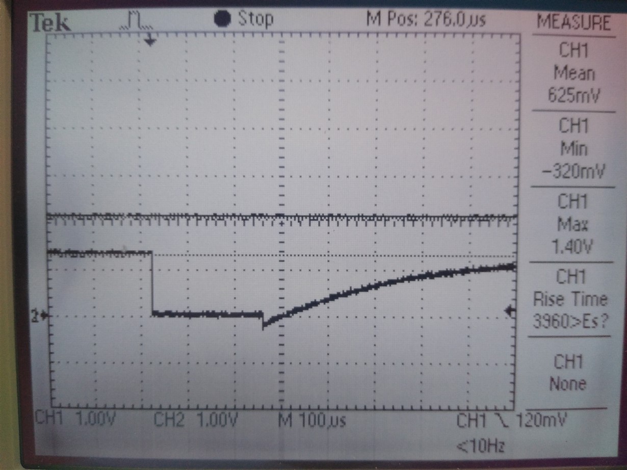
    I finally captured something on the oscilloscope that is suspect.  In can't confirm that this exact EN input pulse caused the voltage regulator to lock up, but I am seeing this pattern consistently on the EN pin.  When it does happen, it happens often and in quick succession (multiple times in under a second).

    I have a pullup resistor on the EN pin.  The high side is attached to VINA (Channel 2 on the scope), and the low side (Channel 1 on the scope) is attached to the EN pin and an NMOS transistor which will pull EN to GND when enabled.  As you can see, we have a situation in which the EN pin will be pulled low for just a few hundred microseconds.  When the NMOS transistor shuts off, the EN pin input bounces down to -320mV prior to climbing back up to 1.4V.

    You should have received schematics and PCB layout at the email address you requested last week.  Could you suggest a modification to remove the negative voltage spike?  After that is fixed we are then going to work on preventing the quick pulses on the EN pin.

    Thanks,

    Bryan

  • Hi Bryan,

    Thanks for all the information, and sorry for the delay. I will look into this and get back to you by end of the day.

    Best regards,
    Milos


  • Milos,

    We figured out the conditions to reliably produce the glitch and then were able to reliably test some fixes.  We added a 1-nF pulldown capacitor on the EN pin and that has seemed to fix the issue.  The no longer see the negative voltage spike and the rise time for the EN line is a few milliseconds longer.  So far we haven't been able to reproduce the problem with the boards that we have added the pulldown capacitor.

    Thanks,

    Bryan

  • Hi Bryan,

    Thanks for the update, and for the detailed explanations which made it easy to understand your circuit.

    In any case I have some additional remarks, which I will send directly by email.

    Best regards,
    Milos