This thread has been locked.

If you have a related question, please click the "Ask a related question" button in the top right corner. The newly created question will be automatically linked to this question.

LM25118-Q1: Maybe camera signal is interferenced by LM25118-Q1 buck boost circuit.

Part Number: LM25118-Q1

Our board is a multi camera aquisition board.

We have a LM25118-Q1 buck boost circuit on Board, when it is working, the camera input signal(Maxim GMSL signal input) is interferened, the images begin to jam.

Can you give some suggestions?

PCB Layout? inductance? capacitance?

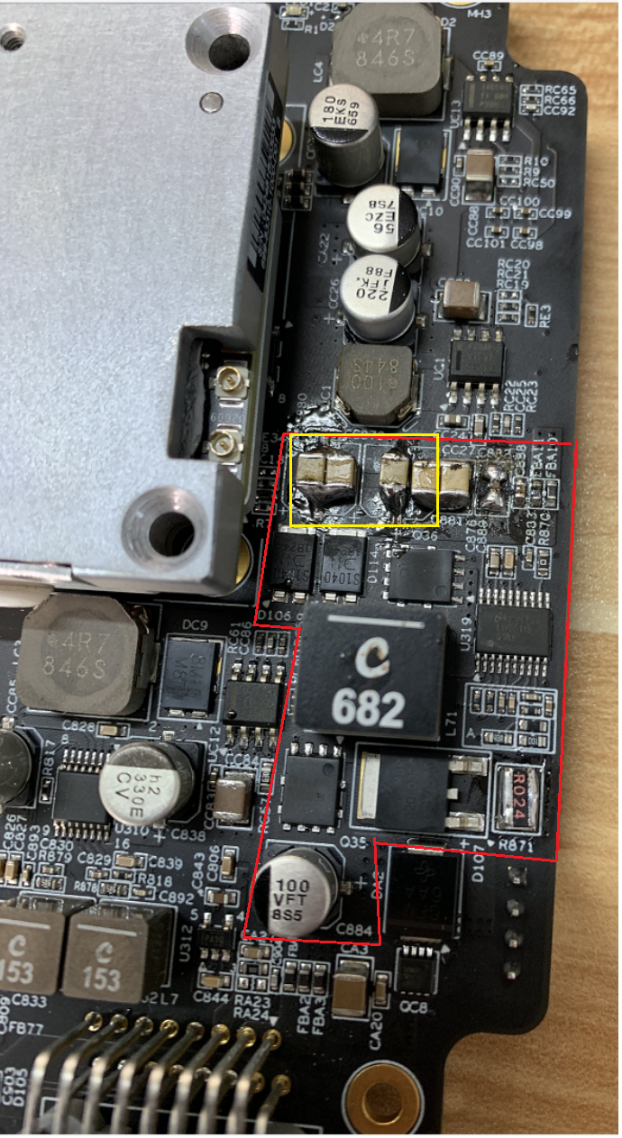
When we replace aluminum capacitance by ceramic capacitance, the camera input signal(image) is stable.

Thanks!

  • Hi User,

    Thank you for posting.  We will study this and get back to you by next Wed.

    Thanks,

    Youhao Xi, Applications Engineering

  • Hi,

    can you give some suggestions?

  • Sorry for the delay.  Not an excuse but we experienced some uncontrollable situations in office this week.

    This seems being related to EMI interference, which is caused by layout. My may try a quick fix by inserting a gate resistor between the MOSFET gate and IC driver pin, which can help slow down the switching transient and reduce the emission. 

    In addition, you may consider to improve your layout. The buck-boost circuit has ac current in both the input side and the output side.  The ac loops are:

    1. Cin --> Buck FET --> SW1 node --> Buck Freewheeling Diode --> Current sense resistor --> Cin ground pin.

    2. MOSFET gate drive signal and the return (back to SW1 for the buck FET, and PGND for boost FET) should be routed closely side by side from the IC pins to the FET, such that the spatial area enclosed by the gate signal loop is minimized.

    3. Cout ground pin --> Boost FET --> SW2 node --> Boost Rectifier Diode --> Cout

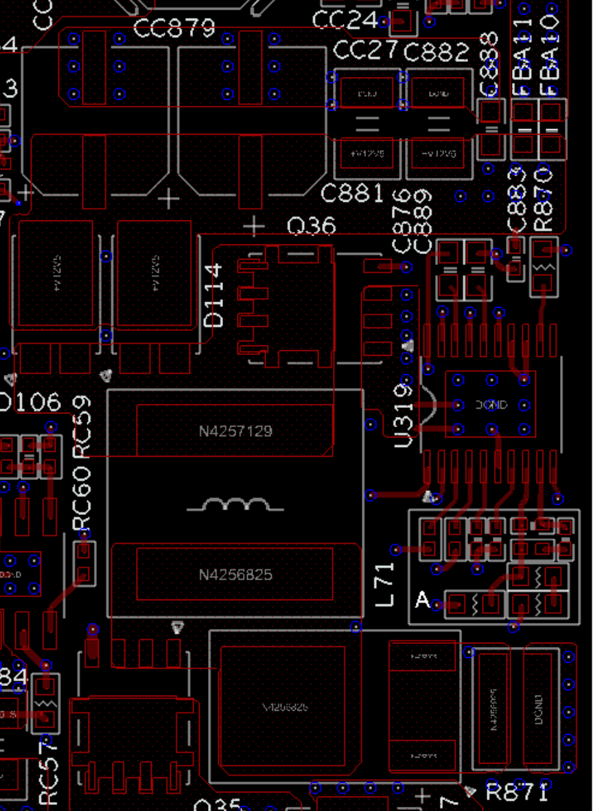
    These two loops must be compact and small, you need to place the part (especially the Cin and Cout) to be close to SW and also route the PCB traces/polygons such that the spatial area enclosed by the ac current loops are minimal. 

    From the pictures of your layout, the buck ac current loop looks large.  The boost ac current loop is not as bad after you placed a few ceramic caps on the position of electrolytic.  However, the Cout bank ground and the Boost FET source should have had direction connection on the surface layer.  

    You may refer to our datasheet layout guidelines, or the EVM layout example, and modify your layout.  

    Since switching power supply is a high EMI generator, please also look into shielding for your camera signals. 

    Thanks,

    Youhao