This thread has been locked.

If you have a related question, please click the "Ask a related question" button in the top right corner. The newly created question will be automatically linked to this question.

BQ24133EVM-715-15V: Help checking and verifying some design issues to track down the cause of failure of some of the IC's on a dozen boards

Part Number: BQ24133EVM-715-15V
Other Parts Discussed in Thread: BQ24133

I have an issue I am trying to track down and need some clarification on a few things regarding the BQ24133 chipset. below is a clip from the circuit I am trying to evaluate that was created by another person.

Question 1) from the below clip is the datasheet that mentions the output capacitance and inductance to keep the device in stability? What does this mean exactly? The circuit that I am evaluating has about 35µF output capacitance and 4.7µH output inductance and by equation 15 means f = 12.4 kHz. what implication will this have?

question 2) is the snubber circuit at the output inductor arranged correctly? I seem to believe the two components are swapped and wouldn't operate the correct way. ( is it even needed?)

question 3) there have been many boards that blow these IC chips for some reason. The hot swapping of the input ( AVCC) never gets above 20 VDC during the transient. To verify that the IC is blown, I probe the SW pin with a scope and see no oscillations. Sometimes the IC has a blown out spot in the lower right corner of the chip near PVCC and the SW pin. The charge current is set to 2A, and the battery voltage is 12.6 V. The stat pin is oscillating at 1 Hz so I know there is a fault but not sure what fault. I tried to diode check (on the board) the internal FET's which appears that the SW pin is shorted to ground indicating a bad FET. What could be causing this to happen. Also, another note of observation is that these chips during charging get almost too hot to touch and there is considerable amount of copper around it. ( enough where I couldn't get the chip off the board with heat on the bottom and top with heat guns). If AVCC is 14.4 then I-ripple is (14.4 *(9V/14.4V)*(1-(9V/14.4V)))/(1600kHz * 4.7µH) = 0.44A. from eq (11) on page 26 of the datasheet. Does this have implication?

Let me know your thoughts.

Thanks,

Justin

  • Hi Justin,

    Regarding 1, the feedback loops (voltage and current) require an LC in a certain range to ensure small signal loop stability.  If unstable, the IC output current or voltage could have a sinusoidal oscillation that is not good for the part.   I am assuming that the capacitors on the board are ceramic.  If so, is their voltage rating at least 1.5 times the expected maximum dc voltage expected on them?  Ceramic capacitors self-derate based on their applied dc voltage.  Therefore having more capacitance is likely not the issue.

    Regarding 2, the snubber looks reasonable.  It is used to minimize EMI from the converter.  You can confirm that it is the not the issue by using an oscilloscope to look at the square waveform at SW.  If the rising and falling edges should only a slight slope and the edges squared off.  If the edges are rounded, then the snubber is sized too large and it is killing efficiency.  If you remove the snubber, do the hot boards cool down?

    Regarding 3, if the internal FET from SW to GND is getting damaged, the most likely cause is overvoltage. Do you have the recommended input snubber to protect against hot plug spikes?  Do you have the external ACFETs installed?  Are there other ICs that use the internal or bottom ground plane (connected from powerpad through vias) for heat sinking and therefore could be saturating your ground plane?

    Regards,

    Jeff

  • 1) The output capacitors are 25V rated so I agree these should be fine.

    2) I will work on getting a screen shot of this. I believe they are rounded slightly. My concern initially was if the resistor and capacitor of the snubber were reversed? If so, will it have the same effect? I will also check if the board gets hot when removed.

    3) Here is the other half of the schematic. The bottom side of the ic has 8 vias connecting to the bottom ground plane. There are no other components on the ground plane on the bottom of the board. The input snubber on the input was modified from the schematic shown below to reduce the transient. I still however believe there is too much capacitance on the input since there is a huge current spike measured on the charger wire ( 44A) measured with a tektronix hall effect probe. The charger has 4mF output capacitance that I measured the other day. For the input snubber I swapped the capacitors with 2 x 22µF and used a 0.5Ω resistor to get the voltage transient measured at the charger input to be less than 20Vdc. The current didn't reduce and I didn't expect it to. However, the voltage transient at AVCC is only about 15 VDC due to the 10 Ω/ 1µF filter. PVCC doesn't see any voltage transient due to the delayed turnon of the ACFET. I suspect that the voltage is not the problem on AVCC but im not sure. The device max spec is 30V if I read that right.

  • Hi Justin,

    Regarding 2, reversing the snubber should not make a difference.

    Regarding 3, I agree about the input capacitance, and the series RC is too large to handle any hotplug events.   4mF on the output is alot but he ACFET should turn on slow enough to help reduce the input current surge.  AVCC is rated for 30V abs max but PVCC and SW are only rated for 20V abs max.  I don't see any other issues with the schematic.   

    Can you measure input current and voltage at plug in and normal operation?

    Regards,

    Jeff

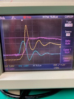
  • Jeff here is a screen view of the input voltage (Yellow), current (blue), and AVCC pin (magenta). The Input voltage and current were measured at the adapter connector just above the snubber. The current was measured with a Textronix TCP2020 (100mV/A) current clamp. The waveform shows about 30V and 48A peak. The charge IC on this unit was blown so the steady state current was zero while the voltage settled at 14.2V which is what the charger adapter is. 

    After doing some more experimenting and talking to a few people, it seems that the IC breaks mostly when quickly unplugging the unit. I have verified that The PVCC pin is turned on 30mS after the adapter is plugged in. 

    Any more thoughts on where to look next,

    Thanks,

    Justin

  • Justin,

    Can you repeat the scope shots but at unplug?  Maybe one of the IC pins is getting pulled more than 1V below ground?

    Regards,

    Jeff

  • The switch pin gets pulled down to -2V when using a spring on the oscilloscope probe to ground. This is when the adapter was plugged in and removed subsequently. What could be the fix to avoid this from happening?

    Thanks,

    Justin

  • Hi Justin,

    You can add a external Schottky diode close to the IC from SW to GND.  This will clamp that voltage to ~ -0.3V below ground.

    Regards,

    Jeff

  • This is the waveform of the -2V spike on the SW pin. Is this even enough to cause the chip to burn up? The duration isn't very long? 

  • Hi Justin,

    Honestly, I wouldn't expect that to damage the device but I don't see anything else wrong with the schematic or layout.

    Jeff

  • I am wondering if there is something that I am not catching on the scope when I am looking at any issues? Or, if there was a bad batch of IC's? Anything is worth looking at I suppose.

  • Hi Justin,

    We haven't had a recent surge in returns for this IC.  But just in case, can you provide the top marking of the failing ICs?  If it there are multiple markings, covering multiple lots, then a bad batch of ICs is likely not the cause.  I can also look at the board layout files.  Can you provide them in pdf format?

    Regards,

    Jeff

  • Hi Justin,

    Any update on this?

    Regards,

    Jeff