This thread has been locked.

If you have a related question, please click the "Ask a related question" button in the top right corner. The newly created question will be automatically linked to this question.

BQ77915: BQ7791500

Part Number: BQ77915

Hello,

I am facing one issue please go through it.

Schematic is attached please collect, 

Whenever there is deep discharge and any cell voltage goes below under-voltage limit DSG MOSFET turns off. and battery voltage appears across the drain to source of DSG MOSFET. 

But according to datasheet CHG MOSFET should remain On with respect to P- terminal, But voltage between gate and source of CHG Mosfet is zero. But there is a voltage of 12V between the gate of CHG Mosfet and B- terminal .
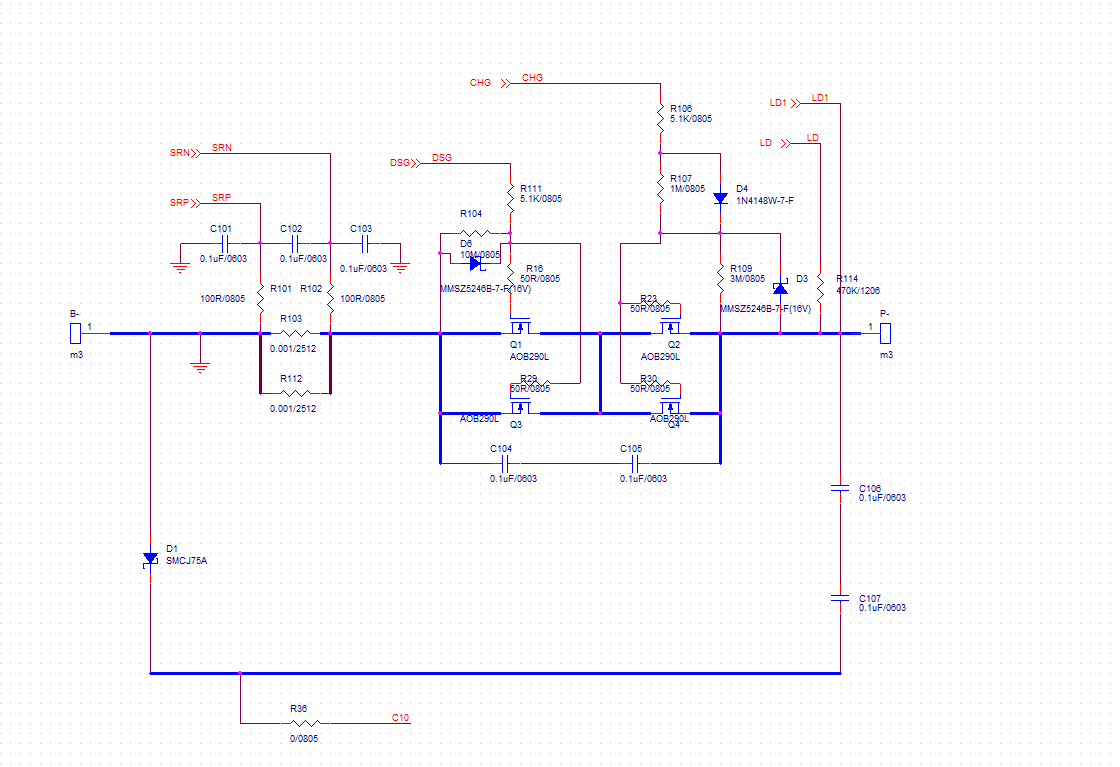
What may be the reason.

  • Hi Gururaj,

    In undervoltage the CHG turns off as shown in table 5 of the data sheet. Charge on level VFETON in the electrical characteristics table is with respect to VSS

    With DSG off, the PACK- pin can be influenced by the the load or the CHG pin voltage as shown in figure 26.

    I did not find a reference of CHG voltage applied with respect to PACK-, please let us know where this is referenced and we can see if we can correct or clarify this in a future document revision.

    Best regards,

    Matt

  • Dear Matt

    PACK- in source or CHG MOSFET whenever  CHG  alone is on voltage should be between gate and source (PACK-) of  CHG MOSFET but there is the voltage across gate and BAT-.

  • Hi Gururaj,

    DSG and CHG output voltage is with respect to VSS which is typically battery-.

    When DSG turns off and PACK- goes high to PACK+, CHG may remain at its high state of 12V.

    As an example if B+ is 15V, VFETON is the regulated 12V.  If DSG is off from UV of a cell, CHG remains on at 12V.  If the load remains on the P+/P- terminals, P+ = P- = 15V  CHG with respect to P- is -3V.  With D3 pulling up the charge gate and D4 blocking most current into the CHG pin, any current which does flow will be in R107.  CHG will not move much. When you measure the gate - source voltage of the charge FETs it will be about 0.  Apply this same analysis to your specific voltages.

    When you remove the load from P+ and P-, the LD pin will pull down on P- and you will see a gate voltage.  The CHG pin will tend to hold up P-, see figure 26 in the BQ77915 data sheet. When the charger voltage is applied, P- is driven down by the charger and the charge FET is on.   At UV recovery the discharge FET turns on and P- is pulled down.