This thread has been locked.

If you have a related question, please click the "Ask a related question" button in the top right corner. The newly created question will be automatically linked to this question.

BQ76PL536A devices do not respond after SLEEP command

We are having a communication issue with a PCB based on the BQ76PL536A. A short time after the stack is put in SLEEP mode, the upper three devices stop replying to SPI communications. The system consists of four BQ76PL536A devices controlled by a C2000 host processor. A reproducible test case is included.

The system properly discovers, configures, and measures all the BQs. However I am unable to communicate with all but the first BQ in the stack after putting them into sleep mode, this includes bringing the BQs out of sleep mode.

Below is a log of the communications between the C2000 and BQ stack. The first test has a long delay (0.5 seconds) after the sleep command which causes all but the first BQ to not respond to a read. The second test is the same except with a shorter delay (10 ms) in this case all BQs still respond.

The only action taken before the following communications is the discovery process that addresses the BQs. The devices have not been flashed with custom OTP configuration. Before each test, power is cycled to the BQ devices.

After devices #2-4 stop replying, issuing a stack reset (7F 3C A5 57) and re-addressing the stack does not cause the upper devices to respond. The only way to re-establish communications with these devices seems to be removing and re-applying power to them.

// 
Test 1

Time [s]	MOSI	MISO	
0		0x00	0x7F	// Broadcast Sleep
8.50833E-05	0x00	0x31
0.000170167	0x00	0x04
0.00025525	0x00	0xD0
				//~0.5 second delay
0.499042833	0x00	0x02	// Read device #1 DEVICE_STATUS register.
0.499127917	0x00	0x00
0.499213	0x00	0x01
0.499298	0xA1	0x00	// Device #1 responds normally.
0.499383083	0x57	0x00
		
0.499680833	0x00	0x04	// Read device #2 DEVICE_STATUS register.
0.499765917	0x00	0x00
0.499851	0x00	0x01	
0.499936	0x00	0x00	// No reply from device #2.
0.500021083	0x00	0x00
		
0.500318833	0x00	0x06	// Read device #3 DEVICE_STATUS register.
0.500403917	0x00	0x00
0.500488917	0x00	0x01
0.500574	0x00	0x00	// No reply.
0.500659083	0x00	0x00
		
0.500956833	0x00	0x08
0.501041917	0x00	0x00
0.501126917	0x00	0x01
0.501212	0x00	0x00
0.501297083	0x00	0x00

Expected behavior: devices reply normally to reads, with valid CRCs.
Observed behavior: devices reply with only 0x00 (invalid CRC).

Test 2

Time [s]	MOSI	MISO
0		0x00	0x7F 	// Broadcast Sleep
8.50833E-05	0x00	0x31
0.000170083	0x00	0x04
0.000255167	0x00	0xD0
				// Delay ~10 ms
0.010989417	0x00	0x02	// Read device #1 DEVICE_STATUS register.
0.0110745	0x00	0x00
0.011159583	0x00	0x01
0.011244583	0xA1	0x00	// Device #1 responds normally.
0.011329667	0x57	0x00
		
0.011627333	0x00	0x04	// Read device #2 DEVICE_STATUS register.
0.011712417	0x00	0x00
0.0117975	0x00	0x01
0.0118825	0xA1	0x00	// Device #2 responds normally.
0.011967583	0x23	0x00
		
0.012265333	0x00	0x06
0.012350333	0x00	0x00
0.012435417	0x00	0x01
0.0125205	0xA1	0x00
0.0126055	0x0F	0x00
		
0.01290325	0x00	0x08
0.012988333	0x00	0x00
0.013073333	0x00	0x01
0.013158417	0xA1	0x00
0.0132435	0xCB	0x00

//
 

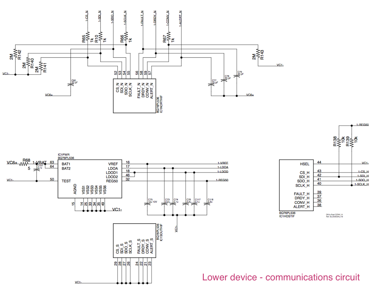
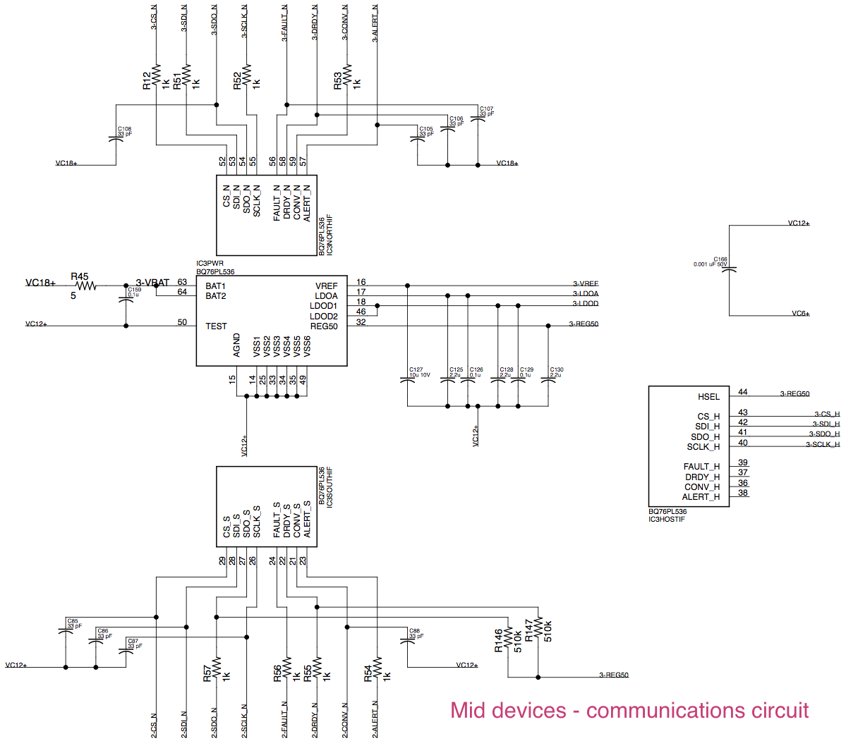
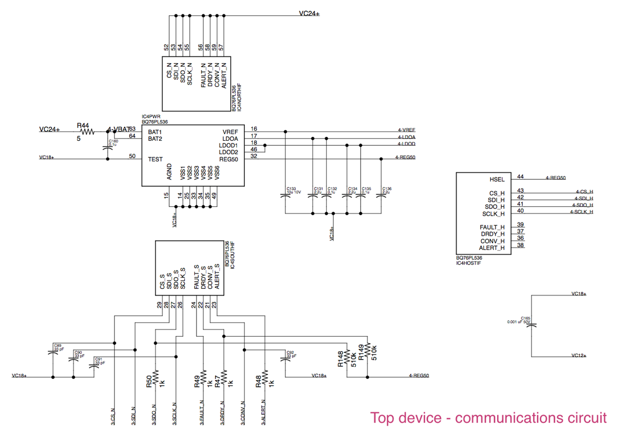
  • Whoops, sorry, I forgot to include the attachments. Here are the schematics and a logic analyzer capture of the communications in question.

  • Aaron,
    10mS and 0.5S shouldn't make difference as long as you asserted and de-sserted /CS properly. I tried with TI gui manually and I know it takes more than 1sec.

    I am wondering the state of /CS pin after 0.5secs delay.

    Find out state of SPI pins with 10mS and 0.5S delay.
  • Aaron,
    It's little hard for me to review the schematic.
    Can you send me your email address?
    I can provide email address for you to send your whole schematic? If you are okay with sending whole schematic.
  • Roger,

    I am working with Aaron on this project. I am doing the Software Aaron is doing the Hardware so we will both be answering your questions. 


    The picture Aaron added to this second reply shows the state of the Serial (MOSI, MISO, CLOCK) and CS pins of the devices during both tests. Do you need more information than the picture provides?

  • Nathan,

    http://www.ti.com/product/BQ76PL536A-Q1/technicaldocuments


    I missed the picture. I didn't know until I zoomed in.

    Goto above link. There is application note on improving communication.

    You will find the relationship between capacitance vs Sclk.

    I know you guys are daisy chaining but don’t know whether they are on same one board or not.

    You guys only have a problem when you have 500mS delay but not with 10mS.

    Do you have scope capture with 10mS delay?

    Have you try without putting IC to sleep mode?

    Datasheet has SPI interface timming and you can reference too.

    Show me the plot when it works and not.

  • Roger,

    I have your email address and will send along the schematic.

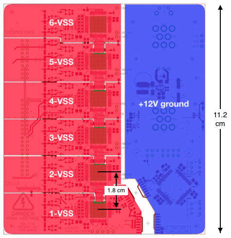
    The devices are on one PCB, with short traces between them (~1-2 cm). I have attached an image which shows the ground planes and spacing of the ICs. We have communicated about this layout before.

    This PCB has been modified to serve as a prototype, so devices #5 and #6 are not populated. North comm lines (SCLK-N, SDO-N, SDI-N, etc) have been terminated to VBAT+ of device 4.

    If the devices are not put in SLEEP mode, they work fine. As far as we can tell, they continue to work indefinitely. We can keep reading and writing to all devices until they are put in SLEEP.

    I'm not sure which signals you would like to see an oscilloscope capture for. What would you like us to measure?

  • Aaron.

    Here is your problem.

    I thought you guys said you were able to communicate with 10mS delay but not with 500mS in sleep mode.

    I don't think 10mS delay won't work either with your schematic.

    Reg50 is disable in sleepmode. You connected HSEL to REG50.

    HSEL is connected to GND for base but not slave.

    You need to connect HSEL to LDOD. Try this then it will work.

    Goto TI site and you can find the schematic reference in the datasheet.

    REMEMBER, REG50 is disable in sleepmode.

  • Roger,

    Thanks for your insight. That seems likely to be the issue - I'm surprised we've missed that for so long. We will modify and test our prototype.

    I think the error probably came from the following note in the datasheet (SLUSAD3A, p. 24):

    Designer Note: Because the LDODx inputs are pulled briefly to ~7 V during programming, the LDODx pins should not be used as sources for pullups to 5-V digital pins, such as HSEL and SPI(bus)_H connected pins. Use VREG50 instead, unless all programming is completed prior to mounting on the application PCB, in which case LDODx is a good choice.

    It seems like this note should be modified to mention that connecting HSEL to VREG50 will prevent the use of SLEEP mode!