This thread has been locked.

If you have a related question, please click the "Ask a related question" button in the top right corner. The newly created question will be automatically linked to this question.

bq21040 waveforms in the datasheet

Other Parts Discussed in Thread: BQ21040

Hello,


Our customer asked me about the condition of the waveforms in bq21040 datasheet.

It is described that the condition is based on typical applications schematic(maybe section 9.2 in page 17),

but in Figure6. Iout shows around 362mA. If the condition is based on section 9.2, so Iout will appear around 540mA, is it correct ?

And please let us know the difference between Vout in Figure3 and Vreg in Fugure 4.

(I think Vout means the voltage at OUT pin, but I have no idea where Vreg is)

Thanks and best regards,
Hiro

  • The data in figure 6 is generated on ATE not from the bench. Therefore, it is not based on the typical application circuit in section 9.2. 

    Figure 4 is miss placed. It is not for this particular part. We will update the datasheet. 

  • Hello Jing-san,

    Thank you for your quick replying, this is very helpful for us.

    I understand and explain it to the customer.

    thanks and best regards,

    Hiro

  • Hello,

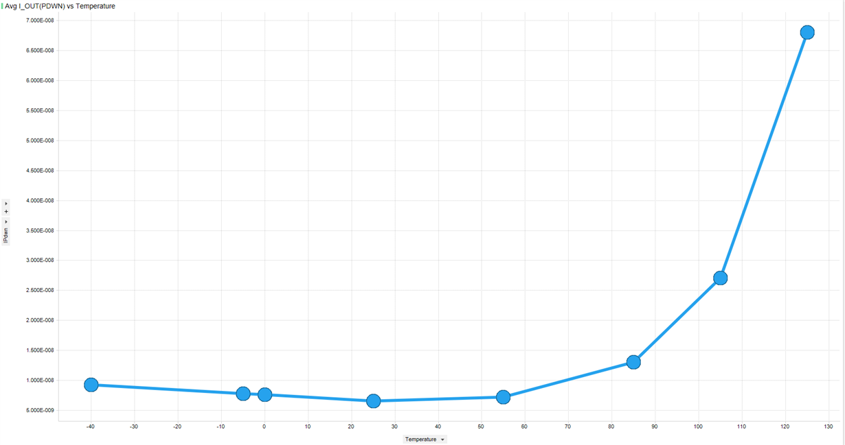
    Could you provide us the information about Iout(pdwn) ?
    It is shown only 1uAmax at over all temperature rannge in the datasheet,
    but our customer wants to know about a tested or estimated value at 0-60degreeC.

    Thanks
    Hiro
  • All test data in the Electrical Characterization table is tested under 0-120 degree C.

  • Hello Jing-san,

    Thank you for your comment.

    I'm sorry for my explanation is not accurate, our customer want to know is

    the actual shutdown current in their operation temperature range. If it is not guaranteed value, it is ok.

    For example, the graph in p.5 "Manual Shutdown Supply Current vs Temperature" in below link is good for them.

    http://cds.linear.com/docs/en/datasheet/406544f.pdf

    (this device is not competitive for bq21040, just for your information)

    Do you have any test result or designed value or information ?

    Thanks and best regards,

    Hiro

  • Hiro-san,

    Please see the plot below.

  • Hello Jing-san,

    Thank you very much for sending this graph, and it looks good for the customer because they are going to select a low Iq device.
    I'll deliver it to the customer.

    Thankis and best regards,
    Hiro
  • Hello Jing-san,

    I got feedback from our customer, please check below.
    Please let us know the conditions of the graph. It seems VIN is 0V, and what is VBAT value ?
    And another reauest is coming,
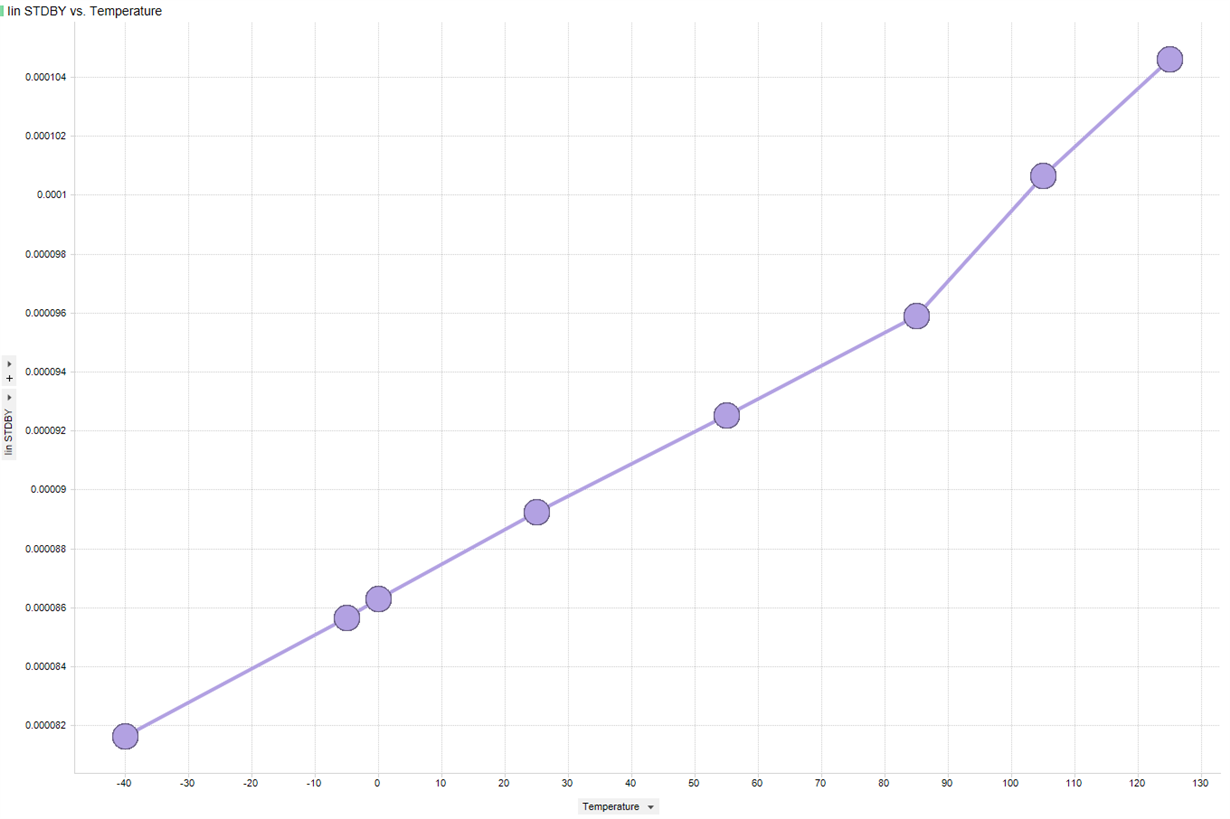
    could you provide graph or data of IIN(STDBY) at 0-60 degreeC ?

    Thanks and best regards,
    Hiro
  • VBAT is at 4.2V for IOUT(PDWN)

    Please see the below plot for IIN(STDBY) over temperature. VIN is 6V.

  • Hello Jing-san,

    Thank you for your sending the graph, this is very helpful for the customer.
    And excuse me for asking frequentry, a new inquiry has come from them.
    It is about the charge temperature.
    In the datasheet section 8.4.5, it is written that above 45 degreeC or below 0 degreeC the charge is disabled.
    Otherwise, in Figure8. , the charge seems also enabled from 45 degreeC to 60 degreeC (4.06V HOT Operation)
    My understandings is that when 10k NTC is connected to TS pin the charge temp is set from 0 to 45 degrees, and
    when a specific setting(I don't know) the charge temp is set from 0 to 60degrees, is it correct ?
    Please let us know the detail for charge temp .

    Thanks and best regards,
    Hiro
  • Your understanding is correct. Please see the foot note at the bottom of figure 8. The JEITA timing does not apply to the bq21040.

  • Hello Jing-san,

    Thank you for your supporting our customer.

    Please let us know about two things.

    1. timer

    30minutes pre-charge timer and 10hours safety timer have not time variation data in the Electrical Characteristics.

    Do you have any reference data or designed value ?

    2. Cts (Optional capacitance-ESD)

    In the Electric Characteristics, typ 0.22uF is shown but there is no other description or figure.

    I think this is used to protect from ESD damage when the battery is connected and this is mounted near the connector like as C5 in the EVM.

    Is it correct ?  If yes, let us know the reason why there is difference 0.1uF(EVM) and 0.22uF(datasheet).

    Thanks and best regards,

    Hiro

  • Hello Jing-san,

    I would be grateful if you could please reply to my query of Sep. 27th.
    Have you had time to look into this ?

    Thanks and best regards,

    Hiro

  • Hiro,

    1.  The timers are based off of an internal oscillator.  We do not specify the internal oscillator. For reference, the oscillator is expected to be within +/-15% across temperature.

    2.  I agree with your assessment that CTS is intended to aid in ESD events since an external battery pack needs the TS pin connection.  I expect the C5 (not populated) in the EVM is mainly for noise reduction on the TS pin to ensure no false temperature events occur.

    Regards,

    Dick

  • Hello Dick-san,

    Thank you for your comment and I understand.

    Our customer waiting for the information, we'll have a meeting as soon as possible.

    Thanks and best regards,

    Hiro