This thread has been locked.

If you have a related question, please click the "Ask a related question" button in the top right corner. The newly created question will be automatically linked to this question.

bq24600 Stand-Alone Synchronous Switch-Mode Li-Ion used to charge 6 cells Li-Ion battery of 7.83Ah capacity with 3A charge current.

Other Parts Discussed in Thread: BQ24600, BQ24650, BQ24616, BQ24610

I would like to know whether bq24600 can be used to charge  6 cells Li-Ion battery of 7.83Ah capacity with 3A charge current or not. I'm using the same circuit mentioned in its datasheet with suitable calculations for 6 cells Li-Ion battery and 3A charge current. The charger circuit is sourced from 28V/3A regulated power supply. But the charger circuit consuming only 130mA from the source. The voltage across battery does not increased  for 2 hours also. please suggest me the suitable application circuit or any changes to be taken. Here I'm attaching the schematic I have used.BATTERY CHARGING SCHEMATIC - 161109.pdf

  • Hi Radha,

    That setup is most definitely within the capabilities of the bq24600.

    It seems like the charger is disabled. Can you measure the charge current (measure the voltage across Rsense), and see if REGN has 6V on it? What is the voltage on SRN with your battery inserted?

    My guess is that the relay is not tripped, keeping the battery disconnected from the charger.
  • Hi David,

    Thank you for your reply. We are getting 6.14V at REGN. The voltage on SRN with battery connected is 22V. For 3A charge current, the inductor value is 3.3uH as you suggested in bq24600 datasheet. But the IC is charging the battery with nearly 1A. When the inductor value is decreased by half the charge current is increased to 2.7A. We also removed the relay and the o/p of charger IC directly connected to battery connector. Why the suggested inductor value 3.3uH not giving the result of 3A. The capacitors used for common mode noise rejection and differential noise elimination in the circuit i.e C10, C11 respectively adds more noise at the sense resistor.

    Thanks & regards
  • Radha,

    Are  you using the same inductor  as the EVM? It could be that for the inductor you are using, the core is saturating, resulting in less charge current. The smaller inductor could have a different b-h curve, which is why the charge current increases.

    The noise is likely layout related. Are the sense lines running through "Noisy" traces/planes? Is the differential filter as close to the IC pins as possible, and the common mode filters close to the sense resistor?

  • Hi,
    I'm using the same inductor as in the EVM. What should I do to get 3A of charge current for 3.3uH inductor? The capacitors are placed as same as you said. But after removing those two capacitors, the pulse across sense resistor is much better when captured in scope. Could you explain the effect of inductor value on charge current and is there any effect on duty cycle of PWM signal here?


    Thanks & regards
  • Radha,

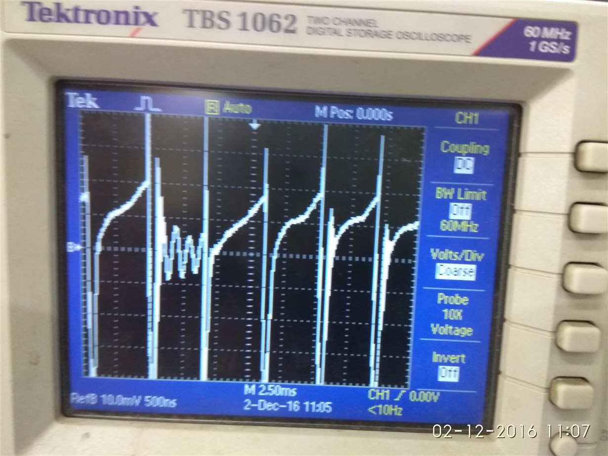
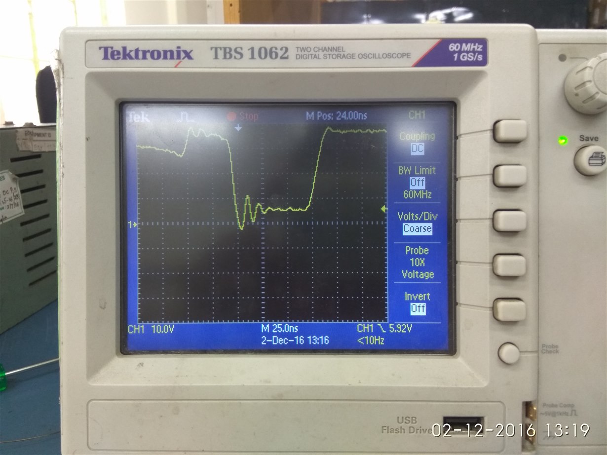
    The inductor plays a role in the small signal modeling of the converter, and would mostly play a role in the load response/stability of the circuit. Could you show me the waveform of the voltage across SRP-SRN?

    Other helpful waveforms would include: SW, VBAT, IBAT(if possible), and Vfb. Have you tested to see if the charge profile as a whole still wokrs? I would look for precharge, fast charge, and termination.... is the output voltage noisy?


    Also, would you mind sharing your layout with me if possible? I have found that many questions similar to yours have been layout related.
  • Hi,

    we could not capture the required screen shots of scope as the Q2 FEt got damaged a few times. And the voltage across C5 capacitor drop at certain events we can't identify the reason. Even if the battery is not getting charged the STAT led is still glowing. We can't find the reasons behind this strange behaviour of IC.

    Thanks & regards

  • Hi,

    I have the development kit of bq24600 and I can't understand what electronic load means. Can I use normal load resistor instead of electronic load?

    Thanks & regards
  • Hi,

    Can I connect the battery across Vbat and Pgnd of J3 connector in EVM?

    Thanks & regards
  • Radha,

    In regards to your EVM questions:

    1) Yes, you should connect your battery + at Vbat, and battery - at PGND

    2) For the  system, you can use a resistive load. However, at Vbat you will need something that more closely resembles a battery. It should be something that is a voltage source that can sink a current. In our labs, we  use electronic loads, bipolar power supplies, or Sourcemeters. You can also do something like this to simulate  a battery: http://www.ti.com/lit/an/slva618/slva618.pdf

    3) Something to note  for the bq24600 EVM is that you should also supply 2V on the TS pin to give the proper bias. If you don't do this, the EVM will be set up to be  in temperature regulation

    In regards to your previous posts:

    1) Could you clarify which traces are which, please?

    2) The voltage  across C5 should not  drop, that  is the  output  of a 6V LDO. The only time this would drop is if VCC is less than 6V

    3) How  did  Q2 fail, and  when? That may provide us some clues as  to what  is happening.

    This is definitely  not expected behavior for the IC, and is  very unusual.

  • Hi,

    The EVM schematic differs from application circuit in datasheet. Is it necessary to follow the same to get best result or we can use simply the application circuit? Could you explain the functional logic of the application circuit?

    1) When we use the EVM for battery charging a constant voltage of 25.15V volts is maintained across Vbat and Pgnd of J3 connector. But in our circuit that follows application circuit, the output voltage never be constant.

    2) Could you explain the reasons that can damage Q2.

    3) The main thing I need to know is as we are getting same values as in EVM, but why the battery not getting charged in the application circuit.

    Thanks & regards
  • Radha,

    Sorry for the delay - we were out for the weekend. I am not sure what you mean by functional logic of the application circuit, but the main difference between the EVM and the datasheet application circuit is the Diode connecting System to Battery. This, in effect, turns the bq24650 into a power path device. With that configuration, battery will power the system when the battery is a diode drop higher than the system.

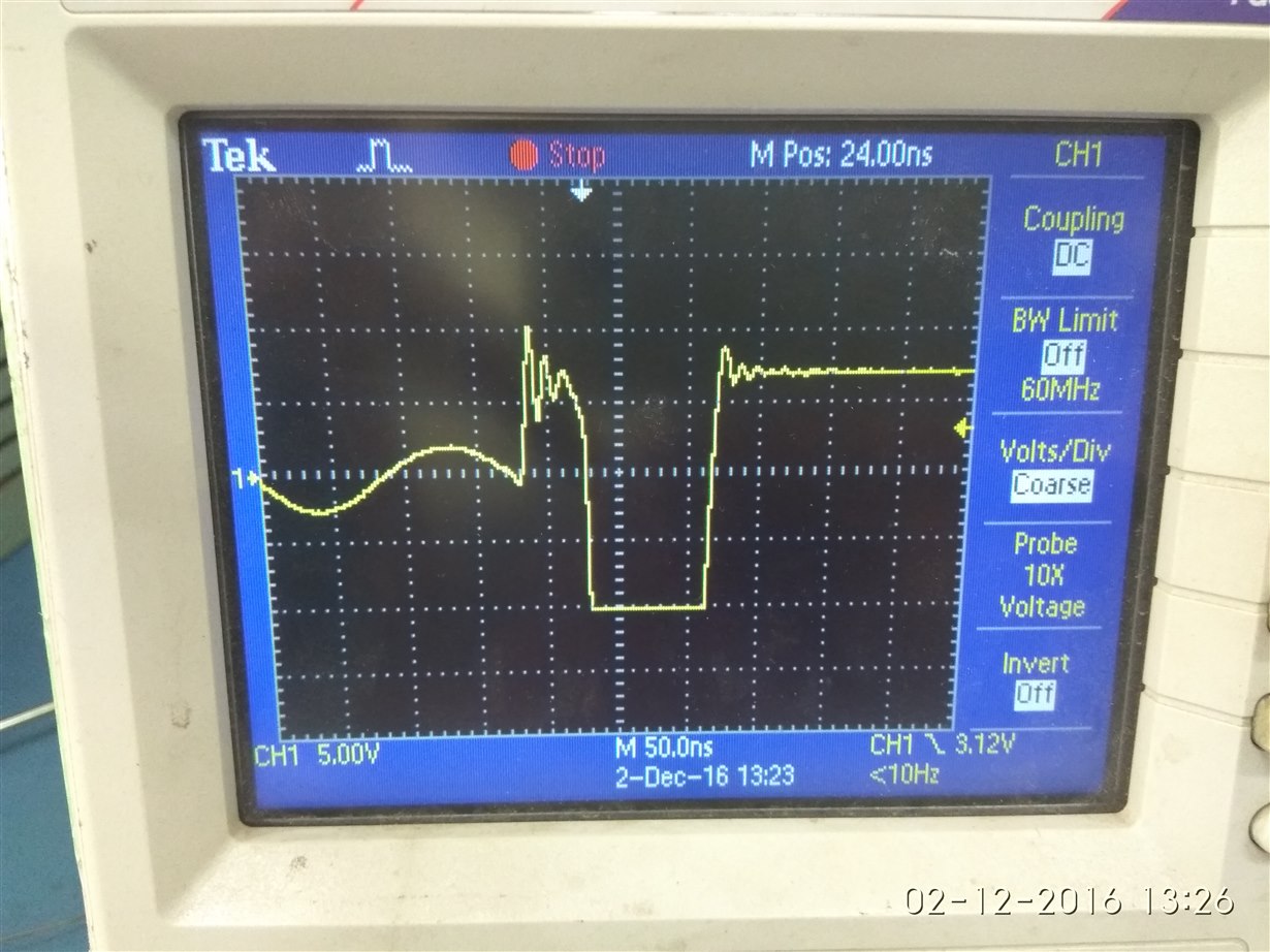
    As far as what could damage Q2 - my guess is an overvoltage or overcurrent condition. If you have a lot of ringing at the switch node, that votlage can couple through the gate and turn on Q2, creating a short from Vin-GND.

    Are you switching the relay circuit at all while charging? If you are dumping charge current into the battery, then take away that connection there will be significant ringing. Can you remove that part of the circuit, and try to only charge the battery? I am guessing you are using the V+ V- connections from the relay to power your system. Removing that will help us narrow things down.
  • Hi,
    I have removed the relay and the output of charging circuit is directly shorted to J1 connector in our board. We have placed the c10, c11 capacitors close to the IC and the output is somewhat better. The battery is charging with 3A with the VCC of 25.6V. But when we increase the VCC more than 25.6V, the charging current decreases rapidly less than 1A. Could you please send the gerber files of bq24600 EVM? I would like to know the working of the bq24600 IC to charge the battery. 

    Thanks & regards

  • You may consider moving to a power path device, so you can remove the relay if that helped. A device such as the bq24610 or bq24616 would work well - they are the same core as the bq24600, but include power path management circuitry.

    All filtering caps should be as close to the IC as possible. From an electrical standpoint, they are on the correct node. Physically, noise can still couple into that node if the caps are far away.

    It sounds like you may have a pretty noisy board. If you have a large amount of ringing, you could be causing the charger to jump into and out of ACOV, causing the effective charging rate to be less. It could also be coupling into SRP/SRN, which will either directly effect charge current, or could cause cycle by cycle overcurrent protection.

    Please send me an email at d-wiest@ti.com and we can handle the GERRBER files offline.
  • Hi,

    I have sent you the modified schematics in mail. Please suggest the component placement and routing for it.


    Thanks & regards
  • Hi,

    Please check the PCB layout and routing that I have sent to you through mail.


    Thanks & regards
  • Hi,

    Could you suggest any specific design lay out for PCB.


    Thanks & regards
  • Hi Radha,

    I had responded with layout feedback over email previously this week. I will resend this email for your convenience.
  • Hi,

    Please suggest the suitable layout and routing for the PCB.

    Thanks & regards
  • Hi Radha,


    If you can place the ground of the output capacitors closer to the ground of the low side switching Fet, I think you will see some improvement. The will redirect the large di/dt loop away from the analog ground of the IC.


    If you want to try and run a small batch with the current layout, it will probably be functional. I have only seen a couple cases where the interference was actually bad enough to cause problems.
  • Hi,

    Could you please provide me the routing for PCB?


    Thanks & regards