This thread has been locked.

If you have a related question, please click the "Ask a related question" button in the top right corner. The newly created question will be automatically linked to this question.

BQ25895: Battery not charging

Part Number: BQ25895

We are working on a design using BQ25895 - The scheme is simple. The load is powered by mains when mains in ON. Battery takes over when mains is OFF. We have connected the load to PMID pin.

The load is approx 2A peak, 700mA average. The adapter (5V source) can supply 3A.

We have tested that the load can be supplied by both mains and using battery boost.

However, the battery is not charging in any condition. There are no faults when reading the I2C registers and the input is being detected as USB DCP = 3.25A.

The registers also indicate charge mode enabled (when mains is available) and device is in fast-charge mode. But both the ADC readings and actual readings show charge current a 0.

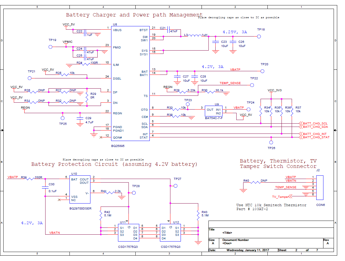
Please see the attached schematic of our design.

We have tried by bypassing the battery protection circuit (bq29700) also. The result is the same.

--

Please help us resolve the issue.

Thanks and Regards,

Saurabh

  • Saurabh, 

    Can you post your I2C register reads here (all registers)? That will give me some insight into what the charger is seeing. 

    Also, you mentioned you have a 700mA load on PMID. Is this present when your VCC_5V is attached? 

    In your schematic, I also see a 3A load on your Vsys pin. Is this load also present? 

    Regards,

    Joel H

  • Please find the PMIC I2C dump below (register address 00 to 14)

    charging
    7F 05 3D 3A 20 13 5E 9D 03 44 93 76 80 15 00 00 00 9A 00 7F 79

    discharging
    7F 05 3D 3A 20 13 5E 9D 03 44 93 E2 80 15 00 00 00 1A 00 3F 39

    --

    The intention of the circuit is as follows:

    We have a 5V 3A adapter that is connected to VBUS input of BQ25895.
    The load (ARM CPU) is connected to PMID pin. The peak power consumption of the load is 2.1A and average consumption is 700mA.
    There is no load connected on SYS pin.

    Case 1: When the adapter is ON, the load is powered by it.
    Case 1.1: The current capacity that remains should be used to charge the battery (we have set max charging limit to ~2A) .
    Case 2: When adapter is off, the battery activated boost mode and powers the load.

    Case 1 and 2 are working as tested in the circuit that we have built.
    Case 1.1, i.e. battery charging is not working.


    Do let me know if you need any more information to help us solve this issue.
  • Hey Saurabh,

    After looking at your I2C dump, it seems like the part is in IINDPM (input current limit). I am not sure why but it seems like you are pulling more current from your input than anticipated through the PMID pin.

    I'm also seeing that the ADC reading for battery voltage and system voltage are too low. I suggest using the 1s Continuous ADC measurement to see what the TS pin %, VBAT voltage, and VSYS voltages are being read by the charger. Is your thermistor also connected during these tests?

    I also suggest checking the SW pin during Case 1/1.1 to check if the part is switching and measure Vsys to make sure it is at minimum.


    Regards,
    Joel H
  • Hi Jeff,

    The logs I have on my PC at present do not have the ADC ON readings, but I had checked the ADC measurements and the VSYS voltage was always fine - 5.2V. I will send you a detailed log in a while. I will also measure the current draw from the adapter using multimeter while taking these readings.

    All the readings had been taken with only a arm cortex M0 micro-controller connected to PMID pin. The micro-controller was used to communicate using I2C. It seems improbable that current limit should have been triggered due to excessive current draw. If you see the log I had sent in this thread earlier, during charging, VBUS voltage is being detected as 5.2V.

    What could be the reason for this condition being triggered?

    I will followup with the detailed set of readings in a while.
  • Please note the detailed readings

    I2C settings (modified from default)
    i2c_write(0x07,0x80); // DISABLE WATCHDOG
    i2c_write(0x02,0x7D); // START ADC READINGS

    Reading 1 : no battery connected - adapter connected on VBUS 5V 2A

    0 1 2 3 4 5 6 7 8 9 a b c d e f 10 11 12 13 14
    7F 05 7D 3A 20 13 5E 80 03 44 93 76 00 15 23 3A 49 9A 00 3F 79
    7F 05 FD 3A 20 13 5E 80 03 44 93 76 00 15 1F 38 49 9A 00 3F 79
    7F 05 7D 3A 20 13 5E 80 03 44 93 76 00 15 1F 38 49 9A 00 3F 79
    7F 05 7D 3A 20 13 5E 80 03 44 93 76 00 15 1F 38 49 9A 00 3F 79
    7F 05 7D 3A 20 13 5E 80 03 44 93 76 00 15 1F 38 49 9A 00 3F 79
    7F 05 7D 3A 20 13 5E 80 03 44 93 76 00 15 1F 38 49 9A 00 3F 79
    7F 05 7D 3A 20 13 5E 80 03 44 93 76 00 15 1F 38 49 9A 00 3F 79
    7F 05 7D 3A 20 13 5E 80 03 44 93 76 00 15 1F 38 49 9A 00 3F 79
    7F 05 7D 3A 20 13 5E 80 03 44 93 76 00 15 27 3A 49 9A 00 7F 79
    7F 05 7D 3A 20 13 5E 80 03 44 93 77 00 15 27 3A 49 9A 00 3F 79
    7F 05 7D 3A 20 13 5E 80 03 44 93 77 00 15 27 3A 49 9A 00 3F 79
    7F 05 7D 3A 20 13 5E 80 03 44 93 77 00 15 27 3A 49 9A 00 7F 79
    7F 05 7D 3A 20 13 5E 80 03 44 93 77 00 15 27 3A 49 9A 00 3F 79
    7F 05 7D 3A 20 13 5E 80 03 44 93 77 00 15 27 3A 49 9A 00 3F 79
    7F 05 7D 3A 20 13 5E 80 03 44 93 77 00 15 27 3A 49 9A 00 3F 79

    -----------------------------


    Reading 2: battery connected - adapter connected on VBUS 5V 2A

    0 1 2 3 4 5 6 7 8 9 a b c d e f 10 11 12 13 14
    7F 05 7D 3A 20 13 5E 80 03 44 93 76 00 15 47 47 49 9A 00 7F 79
    7F 05 7D 3A 20 13 5E 80 03 44 93 76 00 15 47 47 49 9A 00 7F 79
    7F 05 7D 3A 20 13 5E 80 03 44 93 76 00 15 47 47 49 9A 00 7F 79
    7F 05 7D 3A 20 13 5E 80 03 44 93 76 00 15 47 47 49 9A 00 7F 79
    7F 05 7D 3A 20 13 5E 80 03 44 93 76 00 15 47 47 49 9A 00 7F 79
    7F 05 7D 3A 20 13 5E 80 03 44 93 76 00 15 47 47 49 9A 00 7F 79
    7F 05 7D 3A 20 13 5E 80 03 44 93 76 00 15 47 47 49 9A 00 7F 79
    7F 05 7D 3A 20 13 5E 80 03 44 93 76 00 15 47 47 49 9A 00 7F 79
    7F 05 FD 3A 20 13 5E 80 03 44 93 76 00 15 47 47 49 9A 00 7F 79
    7F 05 7D 3A 20 13 5E 80 03 44 93 76 00 15 47 47 49 9A 00 7F 79
    7F 05 7D 3A 20 13 5E 80 03 44 93 76 00 15 47 47 49 9A 00 7F 79
    7F 05 7D 3A 20 13 5E 80 03 44 93 76 00 15 47 47 49 9A 00 7F 79
    7F 05 7D 3A 20 13 5E 80 03 44 93 76 00 15 47 47 49 9A 00 7F 79
    7F 05 7D 3A 20 13 5E 80 03 44 93 76 00 15 47 47 49 9A 00 7F 79

    Total current drawn from power adapter as measured using a multimeter = 36mA

    -----------------------------


    Reading 3: battery connected - adapter connected on VBUS 5V 3A

    0 1 2 3 4 5 6 7 8 9 a b c d e f 10 11 12 13 14
    7F 05 7D 3A 20 13 5E 80 03 44 93 76 00 11 47 47 49 96 00 7F 79
    7F 05 7D 3A 20 13 5E 80 03 44 93 76 00 11 47 47 49 96 00 7F 79
    7F 05 7D 3A 20 13 5E 80 03 44 93 76 00 11 47 47 49 96 00 7F 79
    7F 05 7D 3A 20 13 5E 80 03 44 93 76 00 11 47 47 49 96 00 7F 79
    7F 05 7D 3A 20 13 5E 80 03 44 93 76 00 11 47 47 49 96 00 7F 79
    7F 05 7D 3A 20 13 5E 80 03 44 93 76 00 11 47 47 49 96 00 7F 79
    7F 05 7D 3A 20 13 5E 80 03 44 93 76 00 11 47 47 49 96 00 7F 79
    7F 05 FD 3A 20 13 5E 80 03 44 93 76 00 11 47 47 49 96 00 7F 79
    7F 05 7D 3A 20 13 5E 80 03 44 93 76 00 11 47 47 49 96 00 7F 79
    7F 05 7D 3A 20 13 5E 80 03 44 93 76 00 11 47 47 49 96 00 7F 79
    7F 05 7D 3A 20 13 5E 80 03 44 93 76 00 11 47 47 49 96 00 7F 79
    7F 05 7D 3A 20 13 5E 80 03 44 93 76 00 11 47 47 49 96 00 7F 79
    7F 05 7D 3A 20 13 5E 80 03 44 93 76 00 11 47 47 49 96 00 7F 79
    7F 05 7D 3A 20 13 5E 80 03 44 93 76 00 11 47 47 49 96 00 7F 79
    7F 05 7D 3A 20 13 5E 80 03 44 93 76 00 11 47 47 49 96 00 7F 79

    Total current drawn from power adapter as measured using a multimeter = 28mA

    -----------------------------

    Reading 4: Battery connected - adapter connected on VBUS 5V 3A

    i2c_write(0x07,0x80); // DISABLE WATCHDOG
    i2c_write(0x02,0x6D); // START ADC READINGS & Disable ICO

    0 1 2 3 4 5 6 7 8 9 a b c d e f 10 11 12 13 14
    7F 05 6D 3A 20 13 5E 80 03 44 93 76 00 15 47 47 4A 9A 00 7F 39
    7F 05 6D 3A 20 13 5E 80 03 44 93 76 00 15 47 47 4A 9A 00 7F 39
    7F 05 6D 3A 20 13 5E 80 03 44 93 76 00 15 47 47 4A 9A 00 7F 39
    7F 05 ED 3A 20 13 5E 80 03 44 93 76 00 15 47 47 4A 9A 00 7F 39
    7F 05 6D 3A 20 13 5E 80 03 44 93 76 00 15 47 47 4A 9A 00 7F 39
    7F 05 6D 3A 20 13 5E 80 03 44 93 76 00 15 47 47 4A 9A 00 7F 39
    7F 05 6D 3A 20 13 5E 80 03 44 93 76 00 15 47 47 4A 9A 00 7F 39
    7F 05 6D 3A 20 13 5E 80 03 44 93 76 00 15 47 47 4A 9A 00 7F 39
    7F 05 6D 3A 20 13 5E 80 03 44 93 76 00 15 47 47 4A 9A 00 7F 39
    7F 05 6D 3A 20 13 5E 80 03 44 93 76 00 15 47 47 4A 9A 00 7F 39
    7F 05 6D 3A 20 13 5E 80 03 44 93 76 00 15 47 47 4A 9A 00 7F 39
    7F 05 6D 3A 20 13 5E 80 03 44 93 76 00 15 47 47 4A 9A 00 7F 39
    7F 05 6D 3A 20 13 5E 80 03 44 93 76 00 15 47 47 4A 9A 00 7F 39
    7F 05 6D 3A 20 13 5E 80 03 44 93 76 00 15 47 47 4A 9A 00 7F 39
    7F 05 6D 3A 20 13 5E 80 03 44 93 76 00 15 47 47 4A 9A 00 7F 39

    ------------

    It seems current limit is always triggered no matter what the case.. The actual current draw is actually negligible.

    Please suggest how to move forward.
  • I also tried by Disabling ICO and DCP. The register values are below.

    48 05 60 3A 20 13 5E 80 03 44 93 F6 00 0D 46 46 48 96 00 08 39

    The input and output voltage is set properly. The charger is detected as on-standard 2A adapter. No faults and the device is not in  IINDPM.

    Still charge current is 0.

  • Saurabh,

    In your previous post, the register readings indicate IINDPM mode. Please repeat those conditions but disable ILIM pin (REG00 bit6 =0). Perhaps the wrong ILIM resistor size was installed? The ILIM resistor clamps the input current to its value regardless of the Input Current limit register setting.

    In the most recent post, your registers indicate OTG mode. Was the charger supposed to be in OTG when you read the registers?

    Regards,
    Jeff
  • Hi Jeff,

    We changed the ILIM settings. The charging got started showing a current of 0x03 in the current register.
    We found that the resistor was incorrectly set to 130k instead of 130R.
    Thanks for the pointer in the right direction.

    However, the device seems to be entering VINDPM.
    We have tried setting the REG-0D to 5.3V (0x9B) which is the limit of our supply. Still the result is same - going into VINDPM.
    When it goes in VINDPM, the current becomes 0.

    Can you please elaborate on what VINDPM and INDPM are?
    What settings control these ?

    The load connected is still a STM32 micro-controller which does not draw more than 20mA current.
    The input is a 5V 3A adapter and the input voltage is stable which we have measured.
  • The register values at this time are

    i2c_write(0x07,0x80); // DISABLE WATCHDOG
    i2c_write(0x00,0x30); // DISABLE ILIM PIN
    i2c_write(0x02,0x71); // START ADC READINGS
    i2c_write(0x0D,0x9B); // Set VINDPM


    30 05 71 3A 20 13 5E 80 03 44 93 76 00 9B 4B 4B 4B 97 00 80 39
    30 05 71 3A 20 13 5E 80 03 44 93 76 00 9B 4B 4B 4B 97 00 80 39
    30 05 71 3A 20 13 5E 80 03 44 93 76 00 9B 4B 4B 4B 97 00 80 39
    30 05 71 3A 20 13 5E 80 03 44 93 76 00 9B 4B 4B 4B 97 00 80 39
    30 05 71 3A 20 13 5E 80 03 44 93 76 00 9B 4B 4B 4B 97 00 80 39
    30 05 71 3A 20 13 5E 80 03 44 93 76 00 9B 4B 4B 4B 97 00 80 39
    30 05 71 3A 20 13 5E 80 03 44 93 76 00 9B 4B 4B 4B 97 00 80 39
    30 05 F1 3A 20 13 5E 80 03 44 93 76 00 9B 4B 4B 4B 97 00 80 39
    30 05 71 3A 20 13 5E 80 03 44 93 76 00 9B 4B 4B 4B 97 00 80 39
    30 05 71 3A 20 13 5E 80 03 44 93 76 00 9B 4B 4B 4B 97 00 80 39
    30 05 71 3A 20 13 5E 80 03 44 93 76 00 9B 4B 4B 4B 97 00 80 39
    30 05 71 3A 20 13 5E 80 03 44 93 76 00 9B 4B 4B 4B 97 00 80 39
  • Hey Saurabh,

    I'm glad you were able to find the cause!

    As far as your question regarding VINDPM, this is used when an adapter or power source with unknown power capability is used on VBUS. What this does is prevent the power source from crashing (i.e. the voltage droops out of spec) as it pulls more power than the source can supply. As such, you want to set this to the minimum allowable VBUS voltage. When this voltage is hit as a result of power limitation, the charger will reduce the input current to the charger to maintain that voltage (this is done by reducing the charge current to the battery). 

    IINDPM is for an adapter of which you know the power capability. This sets a current limitation on the charger such that when that input current is detected, the charger also reduces the charge current and limits the input current to that set level. 

    Now your customer has a unique situation, wherein the adapter can provide up to 3A but in reality, the available current to the charger is 3A - 0.700A(nominal) and 3A - 2A(max). So the input current limit (IINLIM register) that should actually be in place should be anywhere from 2.3A to 1A. 

    Based on your register setting, the input current limit is set to 2.5A, meaning the charger will be able to pull up to 2.5A before IINDPM is hit. What would actually happen in a normal VINDPM is that when you are pulling slightly above 2.3A, the voltage on your adapter will start to droop below 5V, until it hits the VINDPM limit.

    However, the VINDPM limit you set (REG 0x0D), set VINDPM = 5.3V) which is already ABOVE VBUS. Therefore the charger cannot reduce the charge current (and therefore the input current) enough to make VBUS rise to 5.3V.

    Change is setting to a lower value as I stated earlier and it should work fine (REG 0x0D). 

    I hope this helps clarify IINDPM and VINDPM. Let me know if you have any more questions.

    Regards,

    Joel H

  • Hi,

    We have checked by reducing the VINDPM and ICHG limits, butthe result is same. Cannot see any charge current.
    And the system still goes in VINDPM.

    The Input Voltage is constant 5.1V at all time - checked on an oscilloscope.
    There is no load connected. We are just checking if battery charging is happening.
    There is some other parameter that is setting the VINDPM.

    i2c_write(0x07,0x80); // - DISABLE WATCHDOG
    i2c_write(0x00,0x30); // - DISABLE ILIM PIN
    I2c_write(0x02,0x79); // - START ADC READINGS
    i2c_write(0x0D,0x96); // - SET VINDPM - REG0D TO 4800mV
    i2c_write(0x04,0x08); // - SET ICHG - REG04 TO 512mA

    30 05 79 3A 08 13 5E 80 03 44 93 76 00 96 4B 4B 4B 96 00 80 39
    30 05 79 3A 08 13 5E 80 03 44 93 76 00 96 4B 4B 4B 96 00 80 39
    30 05 79 3A 08 13 5E 80 03 44 93 76 00 96 4B 4B 4B 96 00 80 39
    30 05 79 3A 08 13 5E 80 03 44 93 76 00 96 4B 4B 4B 96 00 80 39
    30 05 79 3A 08 13 5E 80 03 44 93 76 00 96 4B 4B 4B 96 00 80 39
    30 05 79 3A 08 13 5E 80 03 44 93 76 00 96 4B 4B 4B 96 00 80 39
    30 05 79 3A 08 13 5E 80 03 44 93 76 00 96 4B 4B 4B 96 00 80 39
    30 05 F9 3A 08 13 5E 80 03 44 93 76 00 96 4B 4B 4B 96 00 80 39
    30 05 79 3A 08 13 5E 80 03 44 93 76 00 96 4B 4B 4B 96 00 80 39
    30 05 79 3A 08 13 5E 80 03 44 93 76 00 96 4B 4B 4B 96 00 80 39
    30 05 79 3A 08 13 5E 80 03 44 93 76 00 96 4B 4B 4B 96 00 80 39
    30 05 79 3A 08 13 5E 80 03 44 93 76 00 96 4B 4B 4B 96 00 80 39
    30 05 79 3A 08 13 5E 80 03 44 93 76 00 96 4B 4B 4B 96 00 80 39
  • Hi,

    Update to previous mail. Everything works fine now.

    We restored the registers to original settings and set the ILIM to 2.4A.
    IChg was set to 1A. Watchdog was disabled.

    The charge current is proper.

    Thanks for your help.
  • Hi Joel/Jeff,

    The same circuit as we were discussing in this thread, we implemented on a 2-layer PCB.

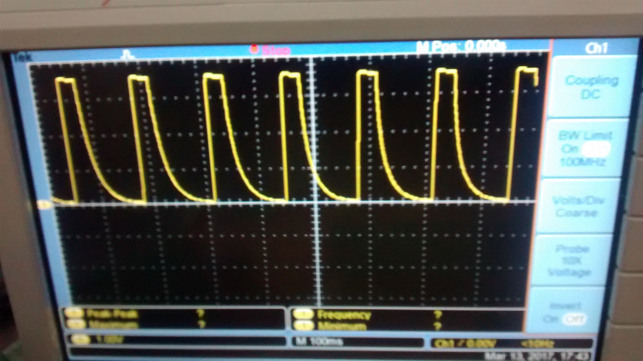
    The Battery charging is working fine but when we remove the VBUS, the REGN pin starts toggling continuously and the VPMID bus voltage also starts toggling.

    On reading the registers, we find that BATFET is disabled.

    WHat could be the reason for this. The schematic is the same as what we checked earlier and everything was working fine.

    Thanks for your help.
  • Hi,

    PFA the schematic that we are testing.

    We have populated only the battery charger IC and related RCs.

    No load is connected. 

    Battery charging is working fine. No problems in that section.

    --

    As soon as we try to go into boost mode, the PMID output stays at 3.5V.

    The resisters indicate that the device does not switch to boost mode.

    The following waveform is observed at the REGN pin. This seems to indicate the device is switching ON and OFF continuously.

    The Serial interface also stops responding after 10-15 replies when we are trying to use boost mode.

    We have also checked by populating same value resistors at the TS pin so as to disable temperature sensor.

    We have crosschecked the values of all components and populated three different boards which are exhibiting same behavior.

    What could be going wrong?

    schematic_ti.pdf

  • Hey Saurabh,

    Sorry for the delay in response.

    Do you have a load attached to VBUS when you try to trigger OTG?

    Could you also put add a channel for VBUS, VBAT, and SW node to investigate further?

    Also, what did you change the PMID capacitor values to? The schematic you sent has some strange numbering for those capacitors.