This thread has been locked.

If you have a related question, please click the "Ask a related question" button in the top right corner. The newly created question will be automatically linked to this question.

BQ24610: BQ24610 and Low side MOS are Burned out when battery plug in

Part Number: BQ24610
Other Parts Discussed in Thread: BQ24650

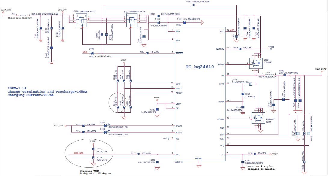
Dear Sir, I attach my schematic. When I plug in the battery(5-series Li battery, the voltage is about 21V), the bq24610(U100), Low side MOS(Q103, connect to LODRV) and Zener Diode(D101, connect to REGN) will be burned out. At this time, the external DC adapter is not pluged in(I do not add the DC_IN_24V). In other words, I just plug in the battery then the bq24610(U100), Low side MOS(Q103) and Zener Diode(D101) are burned out. If  the bq24610(U100), Low side MOS(Q103) and Zener Diode(D101) are not burned out luckly, the charging process can be proceed successfully. The Q103 and bq24610 are grounded to Analog GND. Could you help provide the solution? thanks.

 ) and

  • Could you please upload scope capture when the battery is plugged in? We want to look at the voltage at PH, BTST, and the battery voltage.

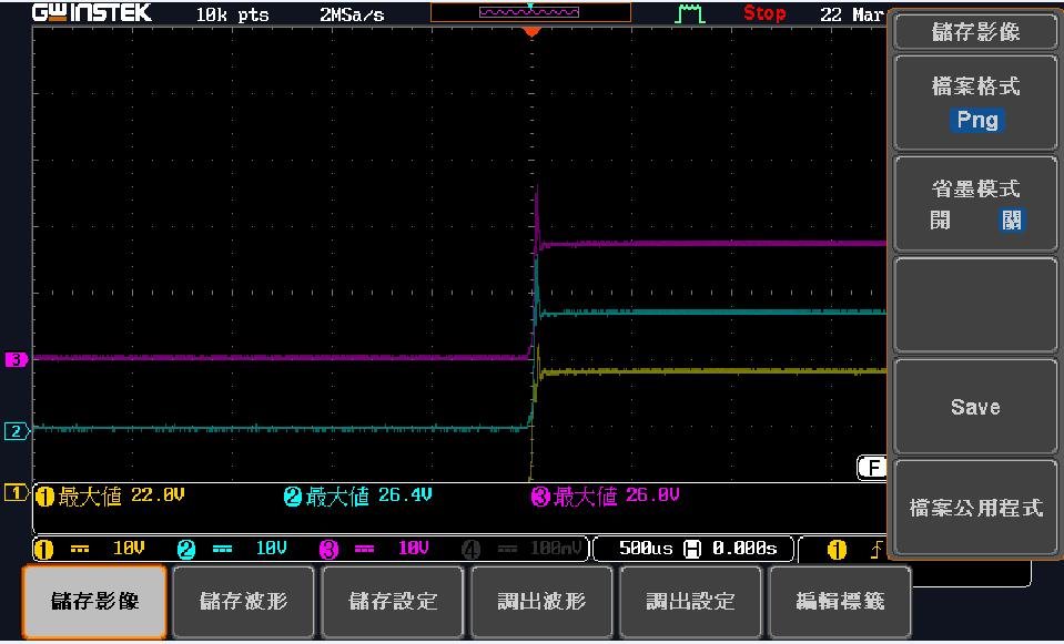
  • Dear Sir, my battery voltage is about 18V. When I plug in the battery, please refer to the waveform . The CH1 is battery voltage. The CH2 is PH voltage. The CH3 

    is BTST voltage. Could you help review my schematic? If you are ok, I will send my schematic to you.

  • Is this captured when the battery plugin damages the low side fet?

    Please send the schematic.


  • Dear Jing, this waveform is From damage PCBA board. I have removed the bq24610 and Low side MOS. The CH1 is battery voltage. The CH2 is PH voltage. The CH3 is BTST voltage. my battery voltage is about 18V. The waveform that I sent to you on 2018/3/22(yesterday) is from normal PCBA. But I has broken 6 pcs PCBA. Could you give me your e-mail? I will send the PDF schematic to you. Thanks.

  • You will need to look at waveform with a board which has both bq24610 and the low side FET on the board, capture the waveform where it get damaged. Not a damaged board without the bq24610 nor the low side FET.

    Assuming this is the waveform is at the damage of the parts, none of these voltages exceed the max rating. The bq24610 has not started up yet when the battery is plugged in. So the low side FET damage  is caused by the action of the battery plug in, not related to bq24610  operation. You may want to contact the MOSFET vander. The rating on the FET is 40V, not sure why it would get damaged with your captured voltage.

    It is possible that Cgd coupling noise which falsely turns on the low side FET cause the damage. Please double check your layout.

  • Dear Jing, I check my damaged board. After I remove the Low side MOS, I measure the PH pin and find it is short to GND. If the MOS's rating is

    insufficient, why the bq24610 PH pin is broken? By the way, why the PH pin voltage always higher than the Battery voltage on my waveform? I search on TI
    E2E, I find the same issue happened on other users. Their waveform is the same with my waveform that PH pin voltage is higher than the battery voltage.
    If bq24610 does not be started when battery plug in, why the PH pin voltage is higher than the battery voltage? Could you suggest any solution to reduce the PH
    pin voltage when battery plug in? Can I add the 100K ohm resistor to GND on MOS's Gate pin(the bq24610 LODRV pin). Maybe due to LODRV pin is turned on
    when battery plug in then the MOS is turned on and it's Drain Pin is shorted to GND? 
    Regards.  
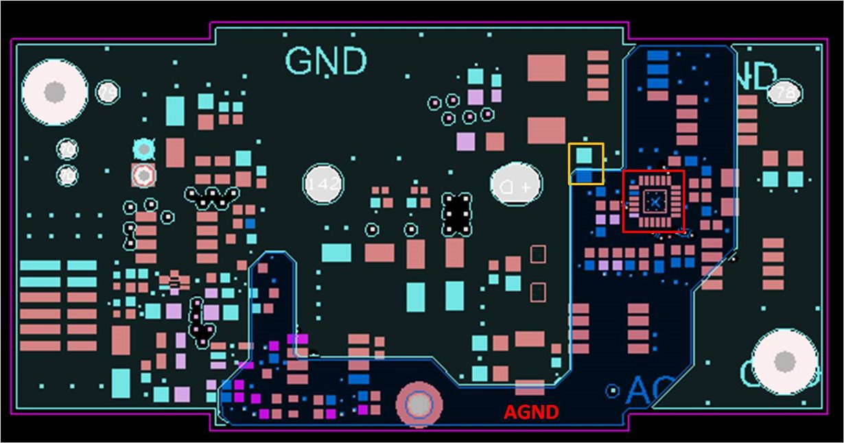
  • Dear Jing, I measure my charging current. It is smaller than my setting. Such as if I set the charging current equal to 900mA, I measure the charging current is about 850mA on TI EVB board. But I measure my PCB board, It is about 780mA(average current on oscilloscope, it's maximum current is about 900mA). What's the root cause? My sense resistor is10 mΩ, the same with TI EVB. Whether I should increase the value of sense resistor? Another issue is the heat of bq24610. When the battery is charging, the bq24610 will heat, but charging can be proceed. Below is my PCB layout, the red block is bq24610, it is mounted on PCB's bottom layer. My PCB is 4-layer. the bq24610's thermal PAD is assigned to AGND on the PCB's second layer(Blue region). The AGND is connected to the PGND via the 0805 0Ω resistor(yellow block). Whether my AGND's area is too smaller to spread out the bq24610's heat? The Taiwan FAE tell me, the heat just will happen on external MOSFET, the bq24610 just is a switching controller and will not be heated. Is this right? Thanks.

  •  Since you are not using battery FET connecting to the system, when battery is plugged in, the current will go through the inductor and the body diode of the high side FET, thus you see the PH node voltage. You can try add a schottky diode from battery to system to help the overshoot on PH pin when battery plug in.

  • Jason, 

    Have you tried with the schottky? Do you still see the failure with the shottky diode?

  • Dear Jing, I have tried the schottky, but the result is failed. I have another question, can I use single GND design on PCBA? Although TI recommend to separate AGND and PGND, but taiwan FAE recommend to use single GND design. I can predict that will reduce the temperature of
    bq24610. Because the bq24610's thermal PAD is defined as AGND, it's area is too small on my PCBA(you can see MAR. 30 issue.).
  • The bq24650 only have one ground. The reason we recommend to use separate AGND and PGND on your layout is that to avoid high power switching noise affect the analog small signal. AGND and PGND eventually join together at the IC.  Looking at your layout capture, I cannot tell if you put solder pad for the thermal pad. Please always solder the thermal pad to the board.

    For the IC damage issue, please submit a FA for further analysis. 

  • Dear Jing, the 17th Pin (GND Pin) of bq24610 should connect to PWR GND or AGND?  The EVB of bq24610 connect the GND pin to PWR GND. Could you tell me whether it is OK? In order to reduce the heat of bq24610, I will connect the thermal pad of bq24610 to PWR GND. Because on my PCBA, the PWR GND area is larger than the AGND. Is this OK?

  • It should be okay to connect to PWR GND. 

  • Dear Jing, Thanks.

  • I have done adding the 1M ohm resistor between Gate pin of low-side MOSFET and GND aiming to keep this MOSFET off (and thus no shoot-through current to damage itself). The result is MOSFET and bq24610 are still damaged.