This thread has been locked.

If you have a related question, please click the "Ask a related question" button in the top right corner. The newly created question will be automatically linked to this question.

bq40z60 Learning Cycle

Other Parts Discussed in Thread: BQ40Z60, BQSTUDIO, BQ2947

We're trying to get our bq40z60 up and running with bqStudio. We're finding it particularly difficult to get the learning cycle going. Is there a "learning cycle guide" available?

The main annoyance is that bqStudio's names for registers do not always line up exactly with the names printed in the reference manual. To make matters even more confusing, the register locations given in the advanced view do not line up with anything that I can find in the reference manual.

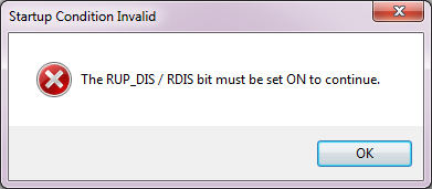
For instance, RDIS must be set to enable the learning cycle. However finding where I can set that register in bqStudio has taken more time that I care to admit and I still struggle to find it on subsequent runs.

Once the learning cycle claims to have started, the output FETs are not enabled. I've been able to enable them in the past with some combination of sending FET_EN, CHG_FET_TOGGLE, and DSG_FET_TOGGLE. Now however even that is not working. It looks like the FUSE output is enabled and preventing DSG/CHG but I cannot figure out why or how to clear it. I've tried sending a "Fuse Toggle" command via 0x001D manually but bqStudio reports communication errors (only for manual SMBus commands).

  • Turnigy 5800mAh 3S 11.1V Battery
  • ~12V VSYS
  • Input: 17V 3A

  • Hello Cameron,

    Sorry for the confusion. Let me review all your concerns above and get back to you in a day or two.

  • Hello Cameron,

    Once you have your board setup, bqStudio and communication verified (seeing cell voltage updates in bqStudio, etc); you're almost ready to start the learning cycle. Click FET_EN button in the Commands tab to enable the CHG and DSG FETs. If you have communication issues in bqStudio, clicking RESET button in the Commands tab help re-establish communication. You will then setup your settings, protection and gauging parameters. R_DIS flag will set until a valid Qmax update is made and a valid OCV reading then it will be clear and Ra table will be updated on subsequent discharge.

    1. Discharge battery to 0% with C/5 to C/10 until Termination Voltage.
    2. Issue a “Reset”.
    3. Wait 30 minutes.
    4. Charge battery to 100% with C/2 to C/10 until taper is reached and valid charge termination is reached.
    5. Wait 2hrs (R_DIS should be cleared during this relax time).
    6. Discharge to 0% with C/5 to C/10 until Termination Voltage (Ra Table should update during this discharge).
    7. Wait 5 hrs.

  • Thank you for your reply. Unfortunately, this does not quite answer my questions and confusions.

    1. It seems FET_EN button/command is really a "toggle" for the FET_EN bit in "Manufacturing Status". I'm assuming you're saying I should ensure the FET_EN bit is set (red box in bqStudio)

    2. Does the learning cycle do software control of the CHG and DSG FET outputs? Some reading suggested you were supposed to use the manual CHG/DSG FET controls for the learning cycle. Please correct me if I'm wrong here.

    3. I'm still unclear on which "settings, protection and gauging parameters" are required to be set before learning. All of the defaults I've found seem sane. I don't know enough about my batteries' limits to tune the settings much better than generic safe LiPo limits. Maybe I'm missing some configuration on this step that is a chip wide FET enable?

    4. I've attempted to follow your instructions and I cannot even get DSG FET output to turn on to start the first step of discharging the battery. I was able to enable the FET in the past so I'm very confident that my hardware setup is correct. My recollection is that bits 1:2 in Operation Status A (CHG and DSG) correspond to the actual FET outputs. I have not been able to switch those bits since the first time that I confirm I was able to. (Something must have changed. At a loss as to what might have.)

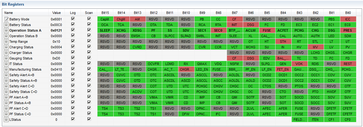
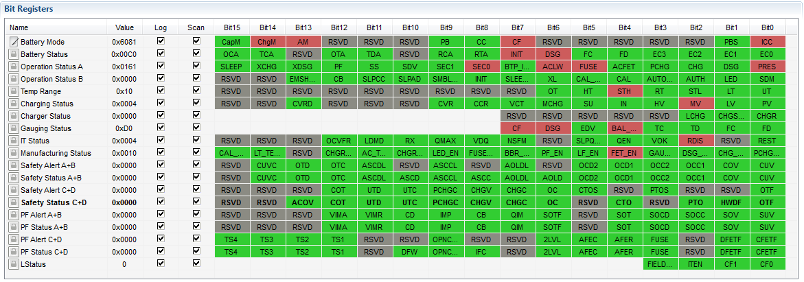
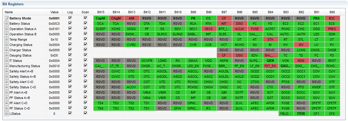
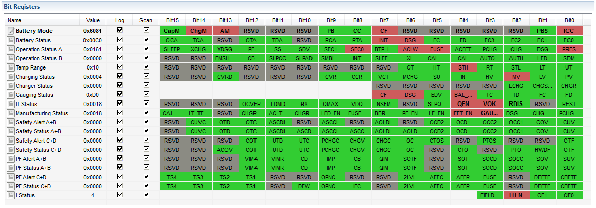
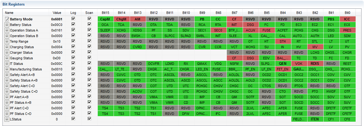
    In the hopes of figuring this out, I'm attempting to document exactly the steps that I've tried. I'm noticing inconsistent behavior after sending "RESET". Not all registers are reset to a known state.

    Cell, pack, and AC voltages detected:

    Initial Registers:

    After sending a RESET:

    After starting learn cycle:

    After sending FET_EN:

    After sending DSG_FET_TOGGLE:

    After sending CHG_FET_TOGGLE:

    After canceling Learn cycle:

    After Reset:

    After FET_EN:

    After Learn Start:

    After Learn Stop:

    After starting Learn again, which won't start because of RDIS bit:

    Repeat start Learn again, no RDIS error:

    At this point, I feel I've tried most combinations that make sense. Any insight would be greatly appreciated.

  • Hello Cameron,

    I feel your frustration. Do you know the charging cut-off voltage, discharge cut-off voltage,  CCCV taper cut-off current and the capacity in mAh for your cells? These should be entered in the protections and Advanced Charge Algorithms portion of the Data Memory tab, if available. You can also start with the defaults. FET_EN should turn on FET_EN bit, but also CHG and DSG bits in Operation Status A register. I take it you're not getting any voltage across VSYS (J5) and PGND. It should be ~11.4V. Do you have a shunt installed on J7 for SYSPRES? If not install one and send a RESET command from bqStudio or go to Data Memory  tab in bqStudio >> Settings >> click DA Configuration >> set NR = 1 then send a RESET command. You should see the voltage on VSYS. This info is in the BQ40z60EVM user's guide in section 4.1. Let me know if this helped.


  • Hello Damian,

    Thank you for the information. Unfortunately, this doesn't seem to work.

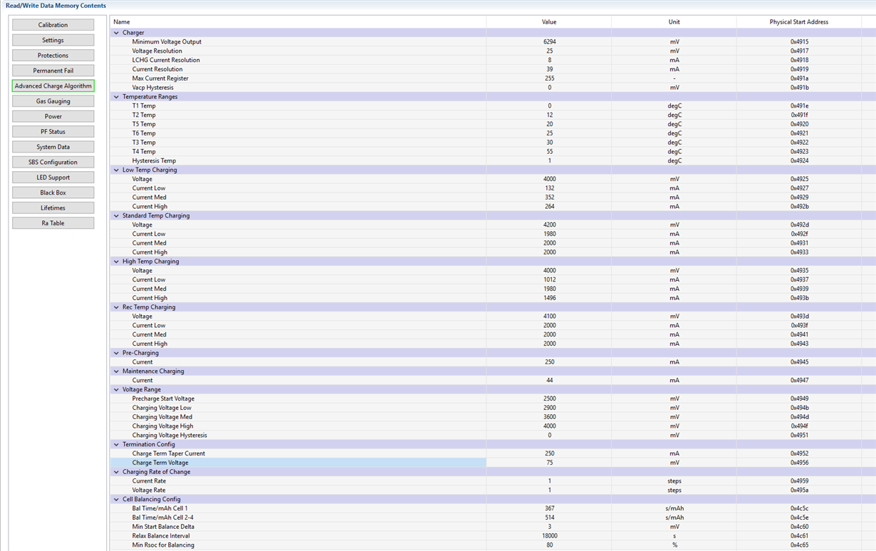
    We are using default values for " cut-off voltage, discharge cut-off voltage,  CCCV taper cut-off current and the capacity" from bq40Z60 for our cells. We have not tried to change those. The default values seem sane to me. The one value that seems like it might be weird is highlighted. But from my reading it looks correct. Please check these if you like:

    Setting the FET_EN bit via FET_EN command does not turn on the DSG and CHG bits as you suggest. This makes me think some hidden fault has been detected. However I haven't found any such faults.

    As is shown in the previous screenshots, PRES bit is set, indicating system is present as far as I can tell and outputs should be enabled. This is because we've set the NR bit.

    Maybe a factory reset command would work? I haven't been able to find such a command.

  • Hi Cameron,

    Sorry, It shouldn't be this difficult. Can you send me a gg.csv file that you can export from Data Memory tab? I'm assuming you're not seeing VSYS output voltage on J5, right? Is the charger connected to the board when doing your checks? The charge (VAC) should be connected in order to wake up the gauge, else you will need to press the WAKE UP button S2 when using only battery.

    charge term voltage is ok at 75mV. It's how close to allow the charging voltage to get within the allowed max battery pack voltage. It's more like a guardband. If you import the srec file for the bq40z60, it will reset the flash to default. Remove the battery and charger. Let sit for 5 mins then reconnect the battery and charger. the device should back to factory default settings.

  • Yes, I'm not seeing voltage on VSYS. I'm also observing the CHG and DSG outputs from the chip and that they stay at or below VBAT thus not turning on.

    VAC is connected. VAC voltage is detected by the bq40z60.

    Good call on the factory reset via firmware update. I will try that now.

    Edit: Forgot to attached .gg.csv (.txt to get around TI block)

    2016-08-22.gg.csv.txt
    * Texas Instruments Data Flash File
    * File created Mon Aug 22 16:18:28 2016
    *
    * Device Number 4600
    * Firmware Version 0.15
    * Build Number 21
    * Order Number 0
    *
    * bqz Device Number 4600
    * bqz Firmware Version 0.15
    * bqz Build Number 21
    *
    * Field Order: Class name, Subclass name, Parameter name, Parameter Value, Display Units
    "Calibration","Voltage","Cell Gain","12101","-"
    "Calibration","Voltage","Pack Gain","49669","-"
    "Calibration","Voltage","BAT Gain","48936","-"
    "Calibration","Current","CC Gain","5.006","mOhm"
    "Calibration","Current","Capacity Gain","5.006","mOhm"
    "Calibration","Current Offset","CC Offset","0","-"
    "Calibration","Current Offset","Coulomb Counter Offset Samples","64","-"
    "Calibration","Current Offset","Board Offset","0","-"
    "Calibration","Current Offset","CC Auto Config","07","hex"
    "Calibration","Current Offset","CC Auto Offset","0","-"
    "Calibration","Temperature","Internal Temp Offset","0","degC"
    "Calibration","Temperature","External1 Temp Offset","0","degC"
    "Calibration","Temperature","External2 Temp Offset","0","degC"
    "Calibration","Temperature","External3 Temp Offset","0","degC"
    "Calibration","Temperature","External4 Temp Offset","0","degC"
    "Calibration","Internal Temp Model","Int Gain","-12143","-"
    "Calibration","Internal Temp Model","Int base offset","6232","-"
    "Calibration","Internal Temp Model","Int Minimum AD","0","-"
    "Calibration","Internal Temp Model","Int Maximum Temp","6232","0.1degK"
    "Calibration","Cell Temperature Model","Coeff a1","-11130","-"
    "Calibration","Cell Temperature Model","Coeff a2","19142","-"
    "Calibration","Cell Temperature Model","Coeff a3","-19262","-"
    "Calibration","Cell Temperature Model","Coeff a4","28203","-"
    "Calibration","Cell Temperature Model","Coeff a5","892","-"
    "Calibration","Cell Temperature Model","Coeff b1","328","-"
    "Calibration","Cell Temperature Model","Coeff b2","-605","-"
    "Calibration","Cell Temperature Model","Coeff b3","-2443","-"
    "Calibration","Cell Temperature Model","Coeff b4","4696","-"
    "Calibration","Cell Temperature Model","Rc0","11703","-"
    "Calibration","Cell Temperature Model","Adc0","11703","-"
    "Calibration","Cell Temperature Model","Rpad","0","-"
    "Calibration","Cell Temperature Model","Rint","0","-"
    "Calibration","Fet Temperature Model","Coeff a1","-11130","-"
    "Calibration","Fet Temperature Model","Coeff a2","19142","-"
    "Calibration","Fet Temperature Model","Coeff a3","-19262","-"
    "Calibration","Fet Temperature Model","Coeff a4","28203","-"
    "Calibration","Fet Temperature Model","Coeff a5","892","-"
    "Calibration","Fet Temperature Model","Coeff b1","328","-"
    "Calibration","Fet Temperature Model","Coeff b2","-605","-"
    "Calibration","Fet Temperature Model","Coeff b3","-2443","-"
    "Calibration","Fet Temperature Model","Coeff b4","4696","-"
    "Calibration","Fet Temperature Model","Rc0","11703","-"
    "Calibration","Fet Temperature Model","Adc0","11703","-"
    "Calibration","Fet Temperature Model","Rpad","0","-"
    "Calibration","Fet Temperature Model","Rint","0","-"
    "Calibration","Current Deadband","Deadband","3","mA"
    "Calibration","Current Deadband","Coulomb Counter Deadband","9","116nV"
    "Settings","Protection","Protection Configuration","00","hex"
    "Settings","Protection","Enabled Protections A","ff","hex"
    "Settings","Protection","Enabled Protections B","7f","hex"
    "Settings","Protection","Enabled Protections C","d5","hex"
    "Settings","Protection","Enabled Protections D","2f","hex"
    "Settings","Permanent Failure","Enabled PF A","00","hex"
    "Settings","Permanent Failure","Enabled PF B","00","hex"
    "Settings","Permanent Failure","Enabled PF C","00","hex"
    "Settings","Permanent Failure","Enabled PF D","00","hex"
    "Settings","Configuration","Charging Configuration","00","hex"
    "Settings","Configuration","Temperature Enable","1f","hex"
    "Settings","Configuration","Temperature Mode","10","hex"
    "Settings","Configuration","DA Configuration","06","hex"
    "Settings","Configuration","FET Options","04","hex"
    "Settings","Configuration","Sbs Gauging Configuration","04","hex"
    "Settings","Configuration","Sbs Configuration","20","hex"
    "Settings","Configuration","Power Config","00","hex"
    "Settings","Configuration","IO Config","81","hex"
    "Settings","Configuration","LED Configuration","00","hex"
    "Settings","Configuration","SOC Flag Config A","0c8c","hex"
    "Settings","Configuration","SOC Flag Config B","8c","hex"
    "Settings","Configuration","Balancing Configuration","03","hex"
    "Settings","Configuration","IT Gauging Configuration","d4fe","hex"
    "Settings","AFE","AFE Protection Control","70","hex"
    "Settings","AFE","ZVCHG Exit Threshold","2200","mV"
    "Settings","Fuse","PF Fuse A","00","hex"
    "Settings","Fuse","PF Fuse B","00","hex"
    "Settings","Fuse","PF Fuse C","00","hex"
    "Settings","Fuse","PF Fuse D","00","hex"
    "Settings","Fuse","Min Blow Fuse Voltage","15000","mV"
    "Settings","Fuse","Fuse Blow Timeout","30","s"
    "Settings","BTP","Init Discharge Set","150","mAH"
    "Settings","BTP","Init Charge Set","175","mAH"
    "Settings","Manufacturing","Mfg Status init","0010","hex"
    "Protections","CUV","Threshold","2500","mV"
    "Protections","CUV","Delay","2","s"
    "Protections","CUV","Recovery","3000","mV"
    "Protections","CUVC","Threshold","2400","mV"
    "Protections","CUVC","Delay","2","s"
    "Protections","CUVC","Recovery","3000","mV"
    "Protections","COV","Threshold Low Temp","4300","mV"
    "Protections","COV","Threshold Standard Temp","4300","mV"
    "Protections","COV","Threshold High Temp","4300","mV"
    "Protections","COV","Threshold Rec Temp","4300","mV"
    "Protections","COV","Delay","2","s"
    "Protections","COV","Recovery Low Temp","3900","mV"
    "Protections","COV","Recovery Standard Temp","3900","mV"
    "Protections","COV","Recovery High Temp","3900","mV"
    "Protections","COV","Recovery Rec Temp","3900","mV"
    "Protections","ACOV","Threshold","20000","mV"
    "Protections","ACOV","Recovery","19000","mV"
    "Protections","OCC1","Threshold","6000","mA"
    "Protections","OCC1","Delay","6","s"
    "Protections","OCC2","Threshold","8000","mA"
    "Protections","OCC2","Delay","3","s"
    "Protections","OCC","Recovery Threshold","-200","mA"
    "Protections","OCC","Recovery Delay","5","s"
    "Protections","OCD1","Threshold","-6000","mA"
    "Protections","OCD1","Delay","6","s"
    "Protections","OCD2","Threshold","-8000","mA"
    "Protections","OCD2","Delay","3","s"
    "Protections","OCD","Recovery Threshold","200","mA"
    "Protections","OCD","Recovery Delay","5","s"
    "Protections","AOLD","Latch Limit","0","-"
    "Protections","AOLD","Counter Dec Delay","10","s"
    "Protections","AOLD","Recovery","5","s"
    "Protections","AOLD","Reset","15","s"
    "Protections","AOLD","Threshold","f4","hex"
    "Protections","ASCC","Latch Limit","0","-"
    "Protections","ASCC","Counter Dec Delay","10","s"
    "Protections","ASCC","Recovery","5","s"
    "Protections","ASCC","Reset","15","s"
    "Protections","ASCC","Threshold","77","hex"
    "Protections","ASCD","Latch Limit","0","-"
    "Protections","ASCD","Counter Dec Delay","10","s"
    "Protections","ASCD","Recovery","5","s"
    "Protections","ASCD","Reset","15","s"
    "Protections","ASCD","Threshold 1","77","hex"
    "Protections","ASCD","Threshold 2","e7","hex"
    "Protections","OTC","Threshold","55.0","1degC"
    "Protections","OTC","Delay","2","s"
    "Protections","OTC","Recovery","50.0","1degC"
    "Protections","OTD","Threshold","60.0","1degC"
    "Protections","OTD","Delay","2","s"
    "Protections","OTD","Recovery","55.0","1degC"
    "Protections","OTF","Threshold","80.0","1degC"
    "Protections","OTF","Delay","2","s"
    "Protections","OTF","Recovery","65.0","1degC"
    "Protections","UTC","Threshold","0","1degC"
    "Protections","UTC","Delay","2","s"
    "Protections","UTC","Recovery","5.0","1degC"
    "Protections","UTD","Threshold","0","1degC"
    "Protections","UTD","Delay","2","s"
    "Protections","UTD","Recovery","5.0","1degC"
    "Protections","COT","Recovery Delay","5","s"
    "Protections","HWD","Delay","10","s"
    "Protections","PTO","Charge Threshold","2000","mA"
    "Protections","PTO","Suspend Threshold","1800","mA"
    "Protections","PTO","Delay","1800","s"
    "Protections","PTO","Reset","2","mAh"
    "Protections","CTO","Charge Threshold","2500","mA"
    "Protections","CTO","Suspend Threshold","2000","mA"
    "Protections","CTO","Delay","54000","s"
    "Protections","CTO","Reset","2","mAh"
    "Protections","OC","Threshold","300","mAh"
    "Protections","OC","Recovery","2","mAh"
    "Protections","OC","RSOC Recovery","90","%"
    "Protections","CHGV","Threshold","500","mV"
    "Protections","CHGV","Delay","30","s"
    "Protections","CHGV","Recovery","-500","mV"
    "Protections","CHGC","Threshold","500","mA"
    "Protections","CHGC","Delay","8","s"
    "Protections","CHGC","Recovery Threshold","100","mA"
    "Protections","CHGC","Recovery Delay","2","s"
    "Protections","PCHGC","Threshold","50","mA"
    "Protections","PCHGC","Delay","2","s"
    "Protections","PCHGC","Recovery Threshold","10","mA"
    "Protections","PCHGC","Recovery Delay","2","s"
    "Permanent Fail","SUV","Threshold","2200","mV"
    "Permanent Fail","SUV","Delay","5","s"
    "Permanent Fail","SOV","Threshold","4500","mV"
    "Permanent Fail","SOV","Delay","5","s"
    "Permanent Fail","SOCC","Threshold","10000","mA"
    "Permanent Fail","SOCC","Delay","5","s"
    "Permanent Fail","SOCD","Threshold","-10000","mA"
    "Permanent Fail","SOCD","Delay","5","s"
    "Permanent Fail","SOT","Threshold","65.0","1degC"
    "Permanent Fail","SOT","Delay","5","s"
    "Permanent Fail","SOTF","Threshold","100.0","1degC"
    "Permanent Fail","SOTF","Delay","5","s"
    "Permanent Fail","Open Thermistor","Threshold","-50.0","1degC"
    "Permanent Fail","Open Thermistor","Delay","5","s"
    "Permanent Fail","Open Thermistor","Fet Delta","20.0","1degC"
    "Permanent Fail","Open Thermistor","Cell Delta","20.0","1degC"
    "Permanent Fail","QIM","Delta Threshold","15.0","%"
    "Permanent Fail","QIM","Delay","2","updates"
    "Permanent Fail","CB","Max Threshold","240","h"
    "Permanent Fail","CB","Delta Threshold","40","h"
    "Permanent Fail","CB","Delay","2","cycles"
    "Permanent Fail","VIMR","Check Voltage","3500","mV"
    "Permanent Fail","VIMR","Check Current","10","mA"
    "Permanent Fail","VIMR","Delta Threshold","500","mV"
    "Permanent Fail","VIMR","Delta Delay","5","s"
    "Permanent Fail","VIMR","Duration","100","s"
    "Permanent Fail","VIMA","Check Voltage","3700","mV"
    "Permanent Fail","VIMA","Check Current","50","mA"
    "Permanent Fail","VIMA","Delta Threshold","200","mV"
    "Permanent Fail","VIMA","Delay","5","s"
    "Permanent Fail","IMP","Delta Threshold","300","%"
    "Permanent Fail","IMP","Max Threshold","400","%"
    "Permanent Fail","IMP","Ra Update Counts","2","counts"
    "Permanent Fail","CD","Threshold","0","mAh"
    "Permanent Fail","CD","Delay","2","cycles"
    "Permanent Fail","CFET","OFF Threshold","5","mA"
    "Permanent Fail","CFET","OFF Delay","5","s"
    "Permanent Fail","DFET","OFF Threshold","-50","mA"
    "Permanent Fail","DFET","OFF Delay","5","s"
    "Permanent Fail","FUSE","Threshold","5","mA"
    "Permanent Fail","FUSE","Delay","5","s"
    "Permanent Fail","AFER","Threshold","100","-"
    "Permanent Fail","AFER","Delay Period","2","s"
    "Permanent Fail","AFER","Compare Period","5","s"
    "Permanent Fail","AFEC","Threshold","100","-"
    "Permanent Fail","AFEC","Delay Period","5","s"
    "Permanent Fail","2LVL","Delay","5","s"
    "Permanent Fail","OPNCELL","Threshold","5000","mV"
    "Permanent Fail","OPNCELL","Delay","5","s"
    "Advanced Charge Algorithm","Charger","Minimum Voltage Output","6294","mV"
    "Advanced Charge Algorithm","Charger","Voltage Resolution","25","mV"
    "Advanced Charge Algorithm","Charger","LCHG Current Resolution","8","mA"
    "Advanced Charge Algorithm","Charger","Current Resolution","39","mA"
    "Advanced Charge Algorithm","Charger","Max Current Register","255","-"
    "Advanced Charge Algorithm","Charger","Vacp Hysteresis","0","mV"
    "Advanced Charge Algorithm","Temperature Ranges","T1 Temp","0","degC"
    "Advanced Charge Algorithm","Temperature Ranges","T2 Temp","12","degC"
    "Advanced Charge Algorithm","Temperature Ranges","T5 Temp","20","degC"
    "Advanced Charge Algorithm","Temperature Ranges","T6 Temp","25","degC"
    "Advanced Charge Algorithm","Temperature Ranges","T3 Temp","30","degC"
    "Advanced Charge Algorithm","Temperature Ranges","T4 Temp","55","degC"
    "Advanced Charge Algorithm","Temperature Ranges","Hysteresis Temp","1","degC"
    "Advanced Charge Algorithm","Low Temp Charging","Voltage","4000","mV"
    "Advanced Charge Algorithm","Low Temp Charging","Current Low","132","mA"
    "Advanced Charge Algorithm","Low Temp Charging","Current Med","352","mA"
    "Advanced Charge Algorithm","Low Temp Charging","Current High","264","mA"
    "Advanced Charge Algorithm","Standard Temp Charging","Voltage","4200","mV"
    "Advanced Charge Algorithm","Standard Temp Charging","Current Low","1980","mA"
    "Advanced Charge Algorithm","Standard Temp Charging","Current Med","2000","mA"
    "Advanced Charge Algorithm","Standard Temp Charging","Current High","2000","mA"
    "Advanced Charge Algorithm","High Temp Charging","Voltage","4000","mV"
    "Advanced Charge Algorithm","High Temp Charging","Current Low","1012","mA"
    "Advanced Charge Algorithm","High Temp Charging","Current Med","1980","mA"
    "Advanced Charge Algorithm","High Temp Charging","Current High","1496","mA"
    "Advanced Charge Algorithm","Rec Temp Charging","Voltage","4100","mV"
    "Advanced Charge Algorithm","Rec Temp Charging","Current Low","2000","mA"
    "Advanced Charge Algorithm","Rec Temp Charging","Current Med","2000","mA"
    "Advanced Charge Algorithm","Rec Temp Charging","Current High","2000","mA"
    "Advanced Charge Algorithm","Pre-Charging","Current","250","mA"
    "Advanced Charge Algorithm","Maintenance Charging","Current","44","mA"
    "Advanced Charge Algorithm","Voltage Range","Precharge Start Voltage","2500","mV"
    "Advanced Charge Algorithm","Voltage Range","Charging Voltage Low","2900","mV"
    "Advanced Charge Algorithm","Voltage Range","Charging Voltage Med","3600","mV"
    "Advanced Charge Algorithm","Voltage Range","Charging Voltage High","4000","mV"
    "Advanced Charge Algorithm","Voltage Range","Charging Voltage Hysteresis","0","mV"
    "Advanced Charge Algorithm","Termination Config","Charge Term Taper Current","250","mA"
    "Advanced Charge Algorithm","Termination Config","Charge Term Voltage","75","mV"
    "Advanced Charge Algorithm","Charging Rate of Change","Current Rate","1","steps"
    "Advanced Charge Algorithm","Charging Rate of Change","Voltage Rate","1","steps"
    "Advanced Charge Algorithm","Cell Balancing Config","Bal Time/mAh Cell 1","367","s/mAh"
    "Advanced Charge Algorithm","Cell Balancing Config","Bal Time/mAh Cell 2-4","514","s/mAh"
    "Advanced Charge Algorithm","Cell Balancing Config","Min Start Balance Delta","3","mV"
    "Advanced Charge Algorithm","Cell Balancing Config","Relax Balance Interval","18000","s"
    "Advanced Charge Algorithm","Cell Balancing Config","Min Rsoc for Balancing","80","%"
    "Gas Gauging","Current Thresholds","Dsg Current Threshold","100","mA"
    "Gas Gauging","Current Thresholds","Chg Current Threshold","50","mA"
    "Gas Gauging","Current Thresholds","Quit Current","10","mA"
    "Gas Gauging","Current Thresholds","Dsg Relax Time","1","s"
    "Gas Gauging","Current Thresholds","Chg Relax Time","60","s"
    "Gas Gauging","Current Thresholds","Dsg Body Diode Protect Threshold","100","mA"
    "Gas Gauging","Current Thresholds","Chg Body Diode Threshold","100","mA"
    "Gas Gauging","Design","Design Capacity mAh","5800","mAh"
    "Gas Gauging","Design","Design Capacity cWh","6336","cWh"
    "Gas Gauging","Design","Design Voltage","10800","mV"
    "Gas Gauging","Cycle","Cycle Count Percentage","90","%"
    "Gas Gauging","FD","Set Voltage Threshold","3000","mV"
    "Gas Gauging","FD","Clear Voltage Threshold","3100","mV"
    "Gas Gauging","FD","Set % RSOC Threshold","0","%"
    "Gas Gauging","FD","Clear % RSOC Threshold","5","%"
    "Gas Gauging","FC","Set Voltage Threshold","4200","mV"
    "Gas Gauging","FC","Clear Voltage Threshold","4100","mV"
    "Gas Gauging","FC","Set % RSOC Threshold","100","%"
    "Gas Gauging","FC","Clear % RSOC Threshold","95","%"
    "Gas Gauging","TD","Set Voltage Threshold","3200","mV"
    "Gas Gauging","TD","Clear Voltage Threshold","3300","mV"
    "Gas Gauging","TD","Set % RSOC Threshold","6","%"
    "Gas Gauging","TD","Clear % RSOC Treshold","8","%"
    "Gas Gauging","TC","Set Voltage Threshold","4200","mV"
    "Gas Gauging","TC","Clear Voltage Threshold","4100","mV"
    "Gas Gauging","TC","Set % RSOC Threshold","100","%"
    "Gas Gauging","TC","Clear % RSOC Threshold","95","%"
    "Gas Gauging","State","Cycle Count","0","-"
    "Gas Gauging","State","Qmax Cell 1","5800","mAh"
    "Gas Gauging","State","Qmax Cell 2","5800","mAh"
    "Gas Gauging","State","Qmax Cell 3","5800","mAh"
    "Gas Gauging","State","Qmax Cell 4","0","mAh"
    "Gas Gauging","State","Qmax Pack","5800","mAh"
    "Gas Gauging","State","Qmax Cycle Count","0","-"
    "Gas Gauging","State","Update Status","00","-"
    "Gas Gauging","State","Cell 1 Chg Voltage at EoC","4200","mV"
    "Gas Gauging","State","Cell 2 Chg Voltage at EoC","4200","mV"
    "Gas Gauging","State","Cell 3 Chg Voltage at EoC","4200","mV"
    "Gas Gauging","State","Cell 4 Chg Voltage at EoC","4200","mV"
    "Gas Gauging","State","Current at EoC","250","mA"
    "Gas Gauging","State","Avg I Last Run","-2000","mA"
    "Gas Gauging","State","Avg P Last Run","-3022","cW"
    "Gas Gauging","State","Delta Voltage","0","mV"
    "Gas Gauging","State","Temp k","1.00","degC/256mW"
    "Gas Gauging","State","Temp a","1000","-"
    "Gas Gauging","State","Max Avg I Last Run","-2000","mA"
    "Gas Gauging","State","Max Avg P Last Run","-3022","cW"
    "Gas Gauging","IT Cfg","Load Select","7","-"
    "Gas Gauging","IT Cfg","Load Mode","0","-"
    "Gas Gauging","IT Cfg","Design Resistance","42","mOhms"
    "Gas Gauging","IT Cfg","User Rate-mA","0","mA"
    "Gas Gauging","IT Cfg","User Rate-cW","0","cW"
    "Gas Gauging","IT Cfg","Reserve Cap-mAh","0","mAh"
    "Gas Gauging","IT Cfg","Reserve Cap-cWh","0","cWh"
    "Gas Gauging","IT Cfg","Pack Resistance","30","mOhms"
    "Gas Gauging","IT Cfg","System Resistance","0","mOhms"
    "Gas Gauging","IT Cfg","Ra Filter","50.0","%"
    "Gas Gauging","IT Cfg","Ra Max Delta","15","%"
    "Gas Gauging","IT Cfg","Reference Grid","4","-"
    "Gas Gauging","IT Cfg","Resistance Parameter Filter","65142","-"
    "Gas Gauging","IT Cfg","Near EDV Ra Param Filter","59220","-"
    "Gas Gauging","IT Cfg","Qmax Delta","5","%"
    "Gas Gauging","IT Cfg","Qmax Upper Bound","130","%"
    "Gas Gauging","IT Cfg","Term Voltage","9000","mV"
    "Gas Gauging","IT Cfg","Term V Hold Time","1","s"
    "Gas Gauging","IT Cfg","Term Voltage Delta","300","mV"
    "Gas Gauging","IT Cfg","Term Min Cell V","2800","mV"
    "Gas Gauging","IT Cfg","Voltage Consistency Delta","300","mV"
    "Gas Gauging","IT Cfg","Fast Scale Start SOC","10","%"
    "Gas Gauging","Smoothing","Smooth Relax Time","1000","s"
    "Gas Gauging","Condition Flag","Max Error Limit","100","%"
    "Gas Gauging","Max Error","Time Cycle Equivalent","24","h"
    "Gas Gauging","Max Error","Cycle Delta","0.05","%"
    "Gas Gauging","SoH","SoH Load Rate","5.0","hour Rate"
    "Gas Gauging","Turbo Cfg","Min Turbo Power","0","cW"
    "Gas Gauging","Turbo Cfg","Max C Rate","-4","C"
    "Gas Gauging","Turbo Cfg","High Frequency Resistance","33","mOhms"
    "Gas Gauging","Turbo Cfg","Reserve Energy %","0","%"
    "Power","Power","Valid Update Voltage","3500","mV"
    "Power","Shutdown","Shutdown Voltage","1750","mV"
    "Power","Shutdown","Shutdown Time","10","s"
    "Power","Shutdown","PF Shutdown Voltage","1750","mV"
    "Power","Shutdown","PF Shutdown Time","10","s"
    "Power","Shutdown","Charger Present Threshold","10000","mV"
    "Power","Sleep","Sleep Current","10","mA"
    "Power","Sleep","Bus Timeout","5","s"
    "Power","Sleep","Voltage Time","5","s"
    "Power","Sleep","Current Time","20","s"
    "Power","Sleep","Wake Comparitor","00","hex"
    "Power","Ship","FET Off Time","10","s"
    "Power","Ship","Delay","20","s"
    "Power","Ship","Auto Ship Time","1440","min"
    "Power","Power Off","Debounce","4","250ms"
    "Power","Power Off","Timeout","30","min"
    "Power","Manual FET Control","MFC Delay","60","s"
    "PF Status","Device Status Data","Safety Alert A","00","hex"
    "PF Status","Device Status Data","Safety Status A","00","hex"
    "PF Status","Device Status Data","Safety Alert B","00","hex"
    "PF Status","Device Status Data","Safety Status B","00","hex"
    "PF Status","Device Status Data","Safety Alert C","00","hex"
    "PF Status","Device Status Data","Safety Status C","00","hex"
    "PF Status","Device Status Data","Safety Alert D","00","hex"
    "PF Status","Device Status Data","Safety Status D","00","hex"
    "PF Status","Device Status Data","PF Alert A","00","hex"
    "PF Status","Device Status Data","PF Status A","00","hex"
    "PF Status","Device Status Data","PF Alert B","00","hex"
    "PF Status","Device Status Data","PF Status B","00","hex"
    "PF Status","Device Status Data","PF Alert C","00","hex"
    "PF Status","Device Status Data","PF Status C","00","hex"
    "PF Status","Device Status Data","PF Alert D","00","hex"
    "PF Status","Device Status Data","PF Status D","00","hex"
    "PF Status","Device Status Data","Fuse Flag","0000","hex"
    "PF Status","Device Status Data","Operation Status A","0000","hex"
    "PF Status","Device Status Data","Operation Status B","0000","hex"
    "PF Status","Device Status Data","Temp Range","00","hex"
    "PF Status","Device Status Data","Charging Status A","00","hex"
    "PF Status","Device Status Data","Charging Status B","00","hex"
    "PF Status","Device Status Data","Charger Status","00","hex"
    "PF Status","Device Status Data","Gauging Status","00","hex"
    "PF Status","Device Status Data","IT Status","0000","hex"
    "PF Status","Device Voltage Data","Cell 1 Voltage","0","mV"
    "PF Status","Device Voltage Data","Cell 2 Voltage","0","mV"
    "PF Status","Device Voltage Data","Cell 3 Voltage","0","mV"
    "PF Status","Device Voltage Data","Cell 4 Voltage","0","mV"
    "PF Status","Device Voltage Data","Battery Direct Voltage","0","mV"
    "PF Status","Device Voltage Data","Pack Voltage","0","mV"
    "PF Status","Device Current Data","Current","0","mA"
    "PF Status","Device Temperature Data","Internal Temperature","-273.2","degC"
    "PF Status","Device Temperature Data","External 1 Temperature","-273.2","degC"
    "PF Status","Device Temperature Data","External 2 Temperature","-273.2","degC"
    "PF Status","Device Temperature Data","External 3 Temperature","-273.2","degC"
    "PF Status","Device Temperature Data","External 4 Temperature","-273.2","degC"
    "PF Status","Device Gauging Data","Cell 1 Dod0","0","-"
    "PF Status","Device Gauging Data","Cell 2 Dod0","0","-"
    "PF Status","Device Gauging Data","Cell 3 Dod0","0","-"
    "PF Status","Device Gauging Data","Cell 4 Dod0","0","-"
    "PF Status","Device Gauging Data","Passed Charge","0","mAh"
    "PF Status","AFE Regs","AFE Interrupt Status","00","hex"
    "PF Status","AFE Regs","AFE FET Status","00","hex"
    "PF Status","AFE Regs","AFE RXIN","00","hex"
    "PF Status","AFE Regs","AFE Latch Status","00","hex"
    "PF Status","AFE Regs","AFE Interrupt Enable","00","hex"
    "PF Status","AFE Regs","AFE FET Control","00","hex"
    "PF Status","AFE Regs","AFE RXIEN","00","hex"
    "PF Status","AFE Regs","AFE RLOUT","00","hex"
    "PF Status","AFE Regs","AFE RHOUT","00","hex"
    "PF Status","AFE Regs","AFE RHINT","00","hex"
    "PF Status","AFE Regs","AFE Cell Balance","00","hex"
    "PF Status","AFE Regs","AFE AD/CC Control","00","hex"
    "PF Status","AFE Regs","AFE ADC Mux","00","hex"
    "PF Status","AFE Regs","AFE LED Output","00","hex"
    "PF Status","AFE Regs","AFE State Control","00","hex"
    "PF Status","AFE Regs","AFE LED/Wake Control","00","hex"
    "PF Status","AFE Regs","AFE Protection Control","00","hex"
    "PF Status","AFE Regs","AFE OCD","00","hex"
    "PF Status","AFE Regs","AFE SCC","00","hex"
    "PF Status","AFE Regs","AFE SCD1","00","hex"
    "PF Status","AFE Regs","AFE SCD2","00","hex"
    "PF Status","AFE Regs","AFE Charger Lock","00",""
    "PF Status","AFE Regs","AFE Charger Voltage","00",""
    "PF Status","AFE Regs","AFE Charger Current","00",""
    "System Data","Manufacturer Data","Manufacturer Info A Length","32","-"
    "System Data","Manufacturer Data","Manufacturer Info Block A01","61","Hex"
    "System Data","Manufacturer Data","Manufacturer Info Block A02","62","Hex"
    "System Data","Manufacturer Data","Manufacturer Info Block A03","63","Hex"
    "System Data","Manufacturer Data","Manufacturer Info Block A04","64","Hex"
    "System Data","Manufacturer Data","Manufacturer Info Block A05","65","Hex"
    "System Data","Manufacturer Data","Manufacturer Info Block A06","66","Hex"
    "System Data","Manufacturer Data","Manufacturer Info Block A07","67","Hex"
    "System Data","Manufacturer Data","Manufacturer Info Block A08","68","Hex"
    "System Data","Manufacturer Data","Manufacturer Info Block A09","69","Hex"
    "System Data","Manufacturer Data","Manufacturer Info Block A10","6a","Hex"
    "System Data","Manufacturer Data","Manufacturer Info Block A11","6b","Hex"
    "System Data","Manufacturer Data","Manufacturer Info Block A12","6c","Hex"
    "System Data","Manufacturer Data","Manufacturer Info Block A13","6d","Hex"
    "System Data","Manufacturer Data","Manufacturer Info Block A14","6e","Hex"
    "System Data","Manufacturer Data","Manufacturer Info Block A15","6f","Hex"
    "System Data","Manufacturer Data","Manufacturer Info Block A16","70","Hex"
    "System Data","Manufacturer Data","Manufacturer Info Block A17","71","Hex"
    "System Data","Manufacturer Data","Manufacturer Info Block A18","72","Hex"
    "System Data","Manufacturer Data","Manufacturer Info Block A19","73","Hex"
    "System Data","Manufacturer Data","Manufacturer Info Block A20","74","Hex"
    "System Data","Manufacturer Data","Manufacturer Info Block A21","75","Hex"
    "System Data","Manufacturer Data","Manufacturer Info Block A22","76","Hex"
    "System Data","Manufacturer Data","Manufacturer Info Block A23","77","Hex"
    "System Data","Manufacturer Data","Manufacturer Info Block A24","7a","Hex"
    "System Data","Manufacturer Data","Manufacturer Info Block A25","78","Hex"
    "System Data","Manufacturer Data","Manufacturer Info Block A26","79","Hex"
    "System Data","Manufacturer Data","Manufacturer Info Block A27","30","Hex"
    "System Data","Manufacturer Data","Manufacturer Info Block A28","31","Hex"
    "System Data","Manufacturer Data","Manufacturer Info Block A29","32","Hex"
    "System Data","Manufacturer Data","Manufacturer Info Block A30","33","Hex"
    "System Data","Manufacturer Data","Manufacturer Info Block A31","34","Hex"
    "System Data","Manufacturer Data","Manufacturer Info Block A32","35","Hex"
    "System Data","Integrity","Static DF Signature","0000","hex"
    "System Data","Integrity","Static Chem DF Signature","6c98","hex"
    "System Data","Integrity","All DF Signature","0000","hex"
    "SBS Configuration","Data","Remaining AH Cap. Alarm","300","mAh"
    "SBS Configuration","Data","Remaining WH Cap. Alarm","432","cWh"
    "SBS Configuration","Data","Remaining Time Alarm","10","min"
    "SBS Configuration","Data","Initial Battery Mode","0081","hex"
    "SBS Configuration","Data","Specification Information","0031","hex"
    "SBS Configuration","Data","Manufacture Date","2016-8-8","date"
    "SBS Configuration","Data","Serial Number","0001","hex"
    "SBS Configuration","Data","Manufacturer Name","Texas Instruments","-"
    "SBS Configuration","Data","Device Name","bq40z60","-"
    "SBS Configuration","Data","Device Chemistry","LION","-"
    "LED Support","LED Config","LED Delay","100","488us"
    "LED Support","LED Config","LED Hold Time","4","s"
    "LED Support","LED Config","CHG Thresh 1","25","%"
    "LED Support","LED Config","CHG Thresh 2","50","%"
    "LED Support","LED Config","CHG Thresh 3","75","%"
    "LED Support","LED Config","CHG Thresh 4","100","%"
    "LED Support","LED Config","DSG Thresh 1","25","%"
    "LED Support","LED Config","DSG Thresh 2","50","%"
    "LED Support","LED Config","DSG Thresh 3","75","%"
    "LED Support","LED Config","DSG Thresh 4","100","%"
    "Black Box","Safety Status","1st Status Status A","00","hex"
    "Black Box","Safety Status","1st Status Status B","00","hex"
    "Black Box","Safety Status","1st Safety Status C","00","hex"
    "Black Box","Safety Status","1st Safety Status D","00","hex"
    "Black Box","Safety Status","1st Time to Next Event","0","s"
    "Black Box","Safety Status","2nd Status Status A","00","hex"
    "Black Box","Safety Status","2nd Status Status B","00","hex"
    "Black Box","Safety Status","2nd Safety Status C","00","hex"
    "Black Box","Safety Status","2nd Safety Status D","00","hex"
    "Black Box","Safety Status","2nd Time to Next Event","0","s"
    "Black Box","Safety Status","3rd Status Status A","00","hex"
    "Black Box","Safety Status","3rd Status Status B","00","hex"
    "Black Box","Safety Status","3rd Safety Status C","00","hex"
    "Black Box","Safety Status","3rd Safety Status D","00","hex"
    "Black Box","Safety Status","3rd Time to Next Event","0","s"
    "Black Box","PF Status","1st PF Status A","00","hex"
    "Black Box","PF Status","1st PF Status B","00","hex"
    "Black Box","PF Status","1st PF Status C","00","hex"
    "Black Box","PF Status","1st PF Status D","00","hex"
    "Black Box","PF Status","1st Time to Next Event","0","s"
    "Black Box","PF Status","2nd PF Status A","00","hex"
    "Black Box","PF Status","2nd PF Status B","00","hex"
    "Black Box","PF Status","2nd PF Status C","00","hex"
    "Black Box","PF Status","2nd PF Status D","00","hex"
    "Black Box","PF Status","2nd Time to Next Event","0","s"
    "Black Box","PF Status","3rd PF Status A","00","hex"
    "Black Box","PF Status","3rd PF Status B","00","hex"
    "Black Box","PF Status","3rd PF Status C","00","hex"
    "Black Box","PF Status","3rd PF Status D","00","hex"
    "Black Box","PF Status","3rd Time to Next Event","0","s"
    "Lifetimes","Voltage","Cell 1 Max Voltage","0","mV"
    "Lifetimes","Voltage","Cell 2 Max Voltage","0","mV"
    "Lifetimes","Voltage","Cell 3 Max Voltage","0","mV"
    "Lifetimes","Voltage","Cell 4 Max Voltage","0","mV"
    "Lifetimes","Voltage","Cell 1 Min Voltage","32767","mV"
    "Lifetimes","Voltage","Cell 2 Min Voltage","32767","mV"
    "Lifetimes","Voltage","Cell 3 Min Voltage","32767","mV"
    "Lifetimes","Voltage","Cell 4 Min Voltage","32767","mV"
    "Lifetimes","Voltage","Max Delta Cell Voltage","0","mV"
    "Lifetimes","Current","Max Charge Current","0","mA"
    "Lifetimes","Current","Max Discharge Current","0","mA"
    "Lifetimes","Current","Max Avg Dsg Current","0","mA"
    "Lifetimes","Current","Max Avg Dsg Power","0","cW"
    "Lifetimes","Temperature","Max Temp Cell","-128","degC"
    "Lifetimes","Temperature","Min Temp Cell","127","degC"
    "Lifetimes","Temperature","Max Delta Cell Temp","0","degC"
    "Lifetimes","Temperature","Max Temp Int Sensor","-128","degC"
    "Lifetimes","Temperature","Min Temp Int Sensor","127","degC"
    "Lifetimes","Temperature","Max Temp Fet","-128","degC"
    "Lifetimes","Safety Events","No Of COV Events","0","events"
    "Lifetimes","Safety Events","Last COV Event","0","cycles"
    "Lifetimes","Safety Events","No Of CUV Events","0","events"
    "Lifetimes","Safety Events","Last CUV Event","0","cycles"
    "Lifetimes","Safety Events","No Of OCD1 Events","0","events"
    "Lifetimes","Safety Events","Last OCD1 Event","0","cycles"
    "Lifetimes","Safety Events","No Of OCD2 Events","0","events"
    "Lifetimes","Safety Events","Last OCD2 Event","0","cycles"
    "Lifetimes","Safety Events","No Of OCC1 Events","0","events"
    "Lifetimes","Safety Events","Last OCC1 Event","0","cycles"
    "Lifetimes","Safety Events","No Of OCC2 Events","0","events"
    "Lifetimes","Safety Events","Last OCC2 Event","0","cycles"
    "Lifetimes","Safety Events","No Of AOLD Events","0","events"
    "Lifetimes","Safety Events","Last AOLD Event","0","cycles"
    "Lifetimes","Safety Events","No Of ASCD Events","0","events"
    "Lifetimes","Safety Events","Last ASCD Event","0","cycles"
    "Lifetimes","Safety Events","No Of ASCC Events","0","events"
    "Lifetimes","Safety Events","Last ASCC Event","0","cycles"
    "Lifetimes","Safety Events","No Of OTC Events","0","events"
    "Lifetimes","Safety Events","Last OTC Event","0","cycles"
    "Lifetimes","Safety Events","No Of OTD Events","0","events"
    "Lifetimes","Safety Events","Last OTD Event","0","cycles"
    "Lifetimes","Safety Events","No Of OTF Events","0","events"
    "Lifetimes","Safety Events","Last OTF Event","0","cycles"
    "Lifetimes","Charging Events","No Valid Charge Term","0","events"
    "Lifetimes","Charging Events","Last Valid Charge Term","0","cycles"
    "Lifetimes","Gauging Events","No Of Qmax Updates","0","events"
    "Lifetimes","Gauging Events","Last Qmax Update","0","cycles"
    "Lifetimes","Gauging Events","No Of Ra Updates","0","events"
    "Lifetimes","Gauging Events","Last Ra Update","0","cycles"
    "Lifetimes","Gauging Events","No Of Ra Disable","0","events"
    "Lifetimes","Gauging Events","Last Ra Disable","0","cycles"
    "Lifetimes","Power Events","No Of Shutdowns","0","events"
    "Lifetimes","Cell Balancing","Cb Time Cell 1","0","h"
    "Lifetimes","Cell Balancing","Cb Time Cell 2","0","h"
    "Lifetimes","Cell Balancing","Cb Time Cell 3","0","h"
    "Lifetimes","Cell Balancing","Cb Time Cell 4","0","h"
    "Lifetimes","Time","Total Fw Runtime","0","h"
    "Lifetimes","Time","Time Spent In UT","0","h"
    "Lifetimes","Time","Time Spent In LT","0","h"
    "Lifetimes","Time","Time Spent In STL","0","h"
    "Lifetimes","Time","Time Spent In RT","0","h"
    "Lifetimes","Time","Time Spent In STH","0","h"
    "Lifetimes","Time","Time Spent In HT","0","h"
    "Lifetimes","Time","Time Spent In OT","0","h"
    "Ra Table","R_a0","Cell0 R_a flag","ff55","-"
    "Ra Table","R_a0","Cell0 R_a 0","67","2^-10ohm"
    "Ra Table","R_a0","Cell0 R_a 1","71","2^-10ohm"
    "Ra Table","R_a0","Cell0 R_a 2","83","2^-10ohm"
    "Ra Table","R_a0","Cell0 R_a 3","110","2^-10ohm"
    "Ra Table","R_a0","Cell0 R_a 4","96","2^-10ohm"
    "Ra Table","R_a0","Cell0 R_a 5","77","2^-10ohm"
    "Ra Table","R_a0","Cell0 R_a 6","96","2^-10ohm"
    "Ra Table","R_a0","Cell0 R_a 7","86","2^-10ohm"
    "Ra Table","R_a0","Cell0 R_a 8","84","2^-10ohm"
    "Ra Table","R_a0","Cell0 R_a 9","82","2^-10ohm"
    "Ra Table","R_a0","Cell0 R_a 10","81","2^-10ohm"
    "Ra Table","R_a0","Cell0 R_a 11","92","2^-10ohm"
    "Ra Table","R_a0","Cell0 R_a 12","103","2^-10ohm"
    "Ra Table","R_a0","Cell0 R_a 13","123","2^-10ohm"
    "Ra Table","R_a0","Cell0 R_a 14","658","2^-10ohm"
    "Ra Table","R_a1","Cell1 R_a flag","ff55","-"
    "Ra Table","R_a1","Cell1 R_a 0","67","2^-10ohm"
    "Ra Table","R_a1","Cell1 R_a 1","71","2^-10ohm"
    "Ra Table","R_a1","Cell1 R_a 2","83","2^-10ohm"
    "Ra Table","R_a1","Cell1 R_a 3","110","2^-10ohm"
    "Ra Table","R_a1","Cell1 R_a 4","96","2^-10ohm"
    "Ra Table","R_a1","Cell1 R_a 5","77","2^-10ohm"
    "Ra Table","R_a1","Cell1 R_a 6","96","2^-10ohm"
    "Ra Table","R_a1","Cell1 R_a 7","86","2^-10ohm"
    "Ra Table","R_a1","Cell1 R_a 8","84","2^-10ohm"
    "Ra Table","R_a1","Cell1 R_a 9","82","2^-10ohm"
    "Ra Table","R_a1","Cell1 R_a 10","81","2^-10ohm"
    "Ra Table","R_a1","Cell1 R_a 11","92","2^-10ohm"
    "Ra Table","R_a1","Cell1 R_a 12","103","2^-10ohm"
    "Ra Table","R_a1","Cell1 R_a 13","123","2^-10ohm"
    "Ra Table","R_a1","Cell1 R_a 14","658","2^-10ohm"
    "Ra Table","R_a2","Cell2 R_a flag","ff55","-"
    "Ra Table","R_a2","Cell2 R_a 0","67","2^-10ohm"
    "Ra Table","R_a2","Cell2 R_a 1","71","2^-10ohm"
    "Ra Table","R_a2","Cell2 R_a 2","83","2^-10ohm"
    "Ra Table","R_a2","Cell2 R_a 3","110","2^-10ohm"
    "Ra Table","R_a2","Cell2 R_a 4","96","2^-10ohm"
    "Ra Table","R_a2","Cell2 R_a 5","77","2^-10ohm"
    "Ra Table","R_a2","Cell2 R_a 6","96","2^-10ohm"
    "Ra Table","R_a2","Cell2 R_a 7","86","2^-10ohm"
    "Ra Table","R_a2","Cell2 R_a 8","84","2^-10ohm"
    "Ra Table","R_a2","Cell2 R_a 9","82","2^-10ohm"
    "Ra Table","R_a2","Cell2 R_a 10","81","2^-10ohm"
    "Ra Table","R_a2","Cell2 R_a 11","92","2^-10ohm"
    "Ra Table","R_a2","Cell2 R_a 12","103","2^-10ohm"
    "Ra Table","R_a2","Cell2 R_a 13","123","2^-10ohm"
    "Ra Table","R_a2","Cell2 R_a 14","658","2^-10ohm"
    "Ra Table","R_a3","Cell3 R_a flag","ff55","-"
    "Ra Table","R_a3","Cell3 R_a 0","67","2^-10ohm"
    "Ra Table","R_a3","Cell3 R_a 1","71","2^-10ohm"
    "Ra Table","R_a3","Cell3 R_a 2","83","2^-10ohm"
    "Ra Table","R_a3","Cell3 R_a 3","110","2^-10ohm"
    "Ra Table","R_a3","Cell3 R_a 4","96","2^-10ohm"
    "Ra Table","R_a3","Cell3 R_a 5","77","2^-10ohm"
    "Ra Table","R_a3","Cell3 R_a 6","96","2^-10ohm"
    "Ra Table","R_a3","Cell3 R_a 7","86","2^-10ohm"
    "Ra Table","R_a3","Cell3 R_a 8","84","2^-10ohm"
    "Ra Table","R_a3","Cell3 R_a 9","82","2^-10ohm"
    "Ra Table","R_a3","Cell3 R_a 10","81","2^-10ohm"
    "Ra Table","R_a3","Cell3 R_a 11","92","2^-10ohm"
    "Ra Table","R_a3","Cell3 R_a 12","103","2^-10ohm"
    "Ra Table","R_a3","Cell3 R_a 13","123","2^-10ohm"
    "Ra Table","R_a3","Cell3 R_a 14","658","2^-10ohm"
    "Ra Table","R_a0x","xCell0 R_a flag","ffff","-"
    "Ra Table","R_a0x","xCell0 R_a 0","67","2^-10ohm"
    "Ra Table","R_a0x","xCell0 R_a 1","71","2^-10ohm"
    "Ra Table","R_a0x","xCell0 R_a 2","83","2^-10ohm"
    "Ra Table","R_a0x","xCell0 R_a 3","110","2^-10ohm"
    "Ra Table","R_a0x","xCell0 R_a 4","96","2^-10ohm"
    "Ra Table","R_a0x","xCell0 R_a 5","77","2^-10ohm"
    "Ra Table","R_a0x","xCell0 R_a 6","96","2^-10ohm"
    "Ra Table","R_a0x","xCell0 R_a 7","86","2^-10ohm"
    "Ra Table","R_a0x","xCell0 R_a 8","84","2^-10ohm"
    "Ra Table","R_a0x","xCell0 R_a 9","82","2^-10ohm"
    "Ra Table","R_a0x","xCell0 R_a 10","81","2^-10ohm"
    "Ra Table","R_a0x","xCell0 R_a 11","92","2^-10ohm"
    "Ra Table","R_a0x","xCell0 R_a 12","103","2^-10ohm"
    "Ra Table","R_a0x","xCell0 R_a 13","123","2^-10ohm"
    "Ra Table","R_a0x","xCell0 R_a 14","658","2^-10ohm"
    "Ra Table","R_a1x","xCell1 R_a flag","ffff","-"
    "Ra Table","R_a1x","xCell1 R_a 0","67","2^-10ohm"
    "Ra Table","R_a1x","xCell1 R_a 1","71","2^-10ohm"
    "Ra Table","R_a1x","xCell1 R_a 2","83","2^-10ohm"
    "Ra Table","R_a1x","xCell1 R_a 3","110","2^-10ohm"
    "Ra Table","R_a1x","xCell1 R_a 4","96","2^-10ohm"
    "Ra Table","R_a1x","xCell1 R_a 5","77","2^-10ohm"
    "Ra Table","R_a1x","xCell1 R_a 6","96","2^-10ohm"
    "Ra Table","R_a1x","xCell1 R_a 7","86","2^-10ohm"
    "Ra Table","R_a1x","xCell1 R_a 8","84","2^-10ohm"
    "Ra Table","R_a1x","xCell1 R_a 9","82","2^-10ohm"
    "Ra Table","R_a1x","xCell1 R_a 10","81","2^-10ohm"
    "Ra Table","R_a1x","xCell1 R_a 11","92","2^-10ohm"
    "Ra Table","R_a1x","xCell1 R_a 12","103","2^-10ohm"
    "Ra Table","R_a1x","xCell1 R_a 13","123","2^-10ohm"
    "Ra Table","R_a1x","xCell1 R_a 14","658","2^-10ohm"
    "Ra Table","R_a2x","xCell2 R_a flag","ffff","-"
    "Ra Table","R_a2x","xCell2 R_a 0","67","2^-10ohm"
    "Ra Table","R_a2x","xCell2 R_a 1","71","2^-10ohm"
    "Ra Table","R_a2x","xCell2 R_a 2","83","2^-10ohm"
    "Ra Table","R_a2x","xCell2 R_a 3","110","2^-10ohm"
    "Ra Table","R_a2x","xCell2 R_a 4","96","2^-10ohm"
    "Ra Table","R_a2x","xCell2 R_a 5","77","2^-10ohm"
    "Ra Table","R_a2x","xCell2 R_a 6","96","2^-10ohm"
    "Ra Table","R_a2x","xCell2 R_a 7","86","2^-10ohm"
    "Ra Table","R_a2x","xCell2 R_a 8","84","2^-10ohm"
    "Ra Table","R_a2x","xCell2 R_a 9","82","2^-10ohm"
    "Ra Table","R_a2x","xCell2 R_a 10","81","2^-10ohm"
    "Ra Table","R_a2x","xCell2 R_a 11","92","2^-10ohm"
    "Ra Table","R_a2x","xCell2 R_a 12","103","2^-10ohm"
    "Ra Table","R_a2x","xCell2 R_a 13","123","2^-10ohm"
    "Ra Table","R_a2x","xCell2 R_a 14","658","2^-10ohm"
    "Ra Table","R_a3x","xCell3 R_a flag","ffff","-"
    "Ra Table","R_a3x","xCell3 R_a 0","67","2^-10ohm"
    "Ra Table","R_a3x","xCell3 R_a 1","71","2^-10ohm"
    "Ra Table","R_a3x","xCell3 R_a 2","83","2^-10ohm"
    "Ra Table","R_a3x","xCell3 R_a 3","110","2^-10ohm"
    "Ra Table","R_a3x","xCell3 R_a 4","96","2^-10ohm"
    "Ra Table","R_a3x","xCell3 R_a 5","77","2^-10ohm"
    "Ra Table","R_a3x","xCell3 R_a 6","96","2^-10ohm"
    "Ra Table","R_a3x","xCell3 R_a 7","86","2^-10ohm"
    "Ra Table","R_a3x","xCell3 R_a 8","84","2^-10ohm"
    "Ra Table","R_a3x","xCell3 R_a 9","82","2^-10ohm"
    "Ra Table","R_a3x","xCell3 R_a 10","81","2^-10ohm"
    "Ra Table","R_a3x","xCell3 R_a 11","92","2^-10ohm"
    "Ra Table","R_a3x","xCell3 R_a 12","103","2^-10ohm"
    "Ra Table","R_a3x","xCell3 R_a 13","123","2^-10ohm"
    "Ra Table","R_a3x","xCell3 R_a 14","658","2^-10ohm"
    

  • You are correct that the FUSE flag will prevent the FETs from turning on. The FUSE pin needs to be connected to VSS, if unused. Check to make sure that it is low.

  • By "FUSE pin" do you mean the AFEFUSE pin? It is connected to ground via 105k ohm in my circuit. I see the EVM schematic uses ~25k. Is this enough of a difference to cause the FUSE bit to trip? This didn't seem to be an issue when this board was first assembled as I've previously been able to enable the FETs.

  • Do you mean the AFEFUSE pin? Is that not an output? Why does its pull-down state matter?

  • Yes, I was referring to the AFEFUSE pin. It is an bidirectional pin that can drive the fuse FET and also detect whether the 2nd level protector device has activated the fuse. It has to be connected to VSS, if unused.

  • By " 2nd level protector device", do you mean the bq2947 that is recommended?

    I have a FET in my circuit to blow a PACK fuse that is connected similarly to the reference design with a 5k ohm fuse coming from each bq device. However for testing, I have disconnected the FET's output so the FUSE doesn't actually blow.

    I see now that the output of the bq2947 is at 3.5V. The AFEFUSE output is at 16.7V. The point driving the FUSE FET is at ~9V. This to me indicates that the AFEFUSE output on the bq40z60 is enabled. Does this correspond to the FUSE bit in Operation Status A? If so, why is the bq40z60 even tripping the fuse? Settings PF Fuse [A-D] are all 0 so my understanding is that it should not ever trip.

    I'm also confused by the "Min Blow Fuse Voltage". There are a couple related settings described in the reference manual but I can't figure out what the intention of this setting is and maybe this is causing the issues.
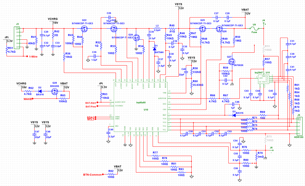
  • Yes, that is the 2nd level protector device. Those are unusual voltage readings. I would not expect the bq2947xx to be 3.5V if the device is driving the output high or low. The AFEFUSE output should only drive up to about 7 or 8V. Can you attach your schematic, so that I can review it?

    The FUSE flag will set, if the device detects that the fuse has been activated to blow. Setting the PF FUSE bits and FUSE_EN = 0 will prevent the gauge from blowing the fuse.

    The "Min Blow Fuse Voltage" is the minimum value for Voltage() that will allow the gauge to try to blow the fuse. there may not be sufficient current to blow the heater in the fuse, if the voltage is lower than this threshold.
  • Is it possible that something has damaged my bq40z60 (or bq2947)? Would that cause these issues?

    The only thing that is not captured in this schematic is the button functionality for waking.

    Q27 is installed but not connected to the FUSE.

  • The circuit implementation for the fuse drive circuit looks correct, but I am concerned about the SN7002. I am not use that it can support the current required to blow the fuse. The FET may be damaged and causing the abnormal voltage readings that you reported. I would try removing the Q27 to see if the voltages return to their normal values. If you do find that the FET is damaged, then check to see how much current rating will be required to support the fuse heater. 

  • While the SN7002 is installed in my circuit, it is not actually connected to the fuse currently. Therefore, I don't believe that could have caused the issue.

    I've removed R67 and connected R66 to ground. As in, OUT on bq2947 is floating, AFEFUSE has a 4.7k ohm path to ground.

    OUT is now at 0V.

    AFEFUSE is at VCHG-0.6V = 17V. I'm worried about shorting AFEFUSE to ground. Is this really necessary?

    Is it possible that the bq40z60 in my circuit is damaged? There is some minor evidence that the bq40z60 got a little hot at some point but I'd attributed it to soldering issues.

  • The device may be damaged, bcecause the output should be low unless a PF is present. I would monitor the AFEFUSE with a scope, disable PF Faults (PF_EN) and send the PF Reset command. (29) See if the signal toggles low. it it does not go low, then the output is probably damaged.

  • By "disable PF Faults (PF_EN)" do you mean send the "PF_EN" "command"? Sending that toggles the "PF_EN" bit in Manufacturing Status. Sending a "PF_CLEAR" command does not have any effect. This make me think we did somehow damage our bq40z60. I will be swapping the chip out soon and checking again.
  • I have replaced the bq40z60 on our circuit. Outputs turn on. It looks like our main issue was a faulty/failed chip.

    I'm still wondering what the full "Getting Started" procedure is. The reported current does not match what my supply and load readouts say. I'm guessing this is because I need to calibrate / input resistance values somewhere. I have not been able to find a guide that explains what is necessary to get accurate readings out. I'm sure that I will have more questions as I get into this.

  • Hello Cameron,

    Glad you're making progress. To get accurate readings from the gauge  setup your gauge parameters for your application, run calibration using bqStudio (this will update based on your Rsense value) , ensure you have the best matched chemID for battery cells by using our GPC tool and run optimization/learning cycle with best match chemID. Note that as the gauge goes through several charge/discharge cycles of the battery (field learning) the accuracy will improved. 

    Most likely the readings you're getting is incorrect because the Rsense value is different. Check Data Memory>>Calibration>> CC gain and Capacity Gain. The default is 5mOhms. Calibration would help correct the value for accuracy or you can manually enter your Rsense value for a quick check. Calibration would be better.

  • Are the DSG & CHG FET outputs supposed to stay on in REST?

    I've managed to get the learning cycle through the discharge stage and into rest. It seemed like the bq40z60 was turning off the DSG output automatically but it might have been the CUV kicking in.

    I'm hoping it does or that manually doing so is ok as I have a ~4mA load on my VSYS that I haven't tracked down yet.
  • Hi Cameron,

    The DSG FET will be disabled during  discharge when a CUV occurs and the CHG FET will be disabled during charging when a COV occurs. Have you done calibration as yet?

  • I have done the calibration but the calibration sets values incorrectly as far as I can tell. Please see this thread where I have described my current calibration woes. I am currently getting readings from the bq40z60 in bqStudio that agree with my meters.

    Are you wondering if the 4mA load is actually an offset calibration issue? It looks like a real load as my cells have lost about 1V over a couple hours.

    I'm worried that this load will affect the rest cycle significantly which is why I'd like DSG to disable. I also don't want to discharge the cells too low.

    Are you suggesting that I set CUV higher so that DSG does turn off and prevent further discharge?

  • Hi Cameron,

    the 4mA current most likely will impact your rest/relaxation cycle, if it causes the dV/dt of the battery to be greater than 1uV/s. That's one criteria for OCV readings needed for Qmax update. I would recommend identifying that current source and resolving it. 

  • I have tried to find the 4mA load. It seems to be drawn by the bq40z60 itself as I've disconnected everything else on VSYS and the load is still there. My dV/dt is around 37 uV/s. I'm considering trying to just send a FET_EN to disable the FETs during the relax cycle. Disabling the DSG fet stops the 4mA current draw. I will then re-enable the FETs at the end of the relax cycle.

    EDIT: Well, that didn't work. RDIS gets cleared and that kills the learning cycle.

  • Hi Cameron,

    Are you getting valid charge termination and full discharge gauging flag settings when running your learning cycle?

  • Hi Cameron,

    What is your Fuse blow FET connected to in your schematic? It doesn't seem to go anywhere. Please send me your GG and log file. I would like to look at your gauge settings and charging voltage. 

  • Hello Damian,

    Yes, my fuse blow FET is not actually connected. We determined that we didn't require that feature, at least for now, but we wanted to at least have the part in the schematic. The FET is populated as shown. It just pulls a point that would otherwise be floating to ground.

    I do not have a full log yet as I still have not been able to run the learning cycle. Attached is the beginning of a cycle.

    I found the 4mA load. An extra resistor was installed that wasn't supposed to be. This created a 2k path to ground from VSYS.

    The latest confusion is that the AC Adapter Voltage is being reported at 10.5V while I can measure it to be ~16V at the ACP (31) and VCC (22) pins.

    I believe the discharge flags are set:

    settings.gg.csv.txt
    * Texas Instruments Data Flash File
    * File created Thu Oct 13 15:27:00 2016
    *
    * Device Number 4600
    * Firmware Version 0.15
    * Build Number 21
    * Order Number 0
    *
    * bqz Device Number 4600
    * bqz Firmware Version 0.15
    * bqz Build Number 21
    *
    * Field Order: Class name, Subclass name, Parameter name, Parameter Value, Display Units
    "Calibration","Voltage","Cell Gain","12136","-"
    "Calibration","Voltage","Pack Gain","33420","-"
    "Calibration","Voltage","BAT Gain","49111","-"
    "Calibration","Current","CC Gain","3.000","mOhm"
    "Calibration","Current","Capacity Gain","10.000","mOhm"
    "Calibration","Current Offset","CC Offset","0","-"
    "Calibration","Current Offset","Coulomb Counter Offset Samples","64","-"
    "Calibration","Current Offset","Board Offset","0","-"
    "Calibration","Current Offset","CC Auto Config","07","hex"
    "Calibration","Current Offset","CC Auto Offset","30","-"
    "Calibration","Temperature","Internal Temp Offset","0","degC"
    "Calibration","Temperature","External1 Temp Offset","0","degC"
    "Calibration","Temperature","External2 Temp Offset","0","degC"
    "Calibration","Temperature","External3 Temp Offset","0","degC"
    "Calibration","Temperature","External4 Temp Offset","0","degC"
    "Calibration","Internal Temp Model","Int Gain","-12143","-"
    "Calibration","Internal Temp Model","Int base offset","6232","-"
    "Calibration","Internal Temp Model","Int Minimum AD","0","-"
    "Calibration","Internal Temp Model","Int Maximum Temp","6232","0.1degK"
    "Calibration","Cell Temperature Model","Coeff a1","-11130","-"
    "Calibration","Cell Temperature Model","Coeff a2","19142","-"
    "Calibration","Cell Temperature Model","Coeff a3","-19262","-"
    "Calibration","Cell Temperature Model","Coeff a4","28203","-"
    "Calibration","Cell Temperature Model","Coeff a5","892","-"
    "Calibration","Cell Temperature Model","Coeff b1","328","-"
    "Calibration","Cell Temperature Model","Coeff b2","-605","-"
    "Calibration","Cell Temperature Model","Coeff b3","-2443","-"
    "Calibration","Cell Temperature Model","Coeff b4","4696","-"
    "Calibration","Cell Temperature Model","Rc0","11703","-"
    "Calibration","Cell Temperature Model","Adc0","11703","-"
    "Calibration","Cell Temperature Model","Rpad","0","-"
    "Calibration","Cell Temperature Model","Rint","0","-"
    "Calibration","Fet Temperature Model","Coeff a1","-11130","-"
    "Calibration","Fet Temperature Model","Coeff a2","19142","-"
    "Calibration","Fet Temperature Model","Coeff a3","-19262","-"
    "Calibration","Fet Temperature Model","Coeff a4","28203","-"
    "Calibration","Fet Temperature Model","Coeff a5","892","-"
    "Calibration","Fet Temperature Model","Coeff b1","328","-"
    "Calibration","Fet Temperature Model","Coeff b2","-605","-"
    "Calibration","Fet Temperature Model","Coeff b3","-2443","-"
    "Calibration","Fet Temperature Model","Coeff b4","4696","-"
    "Calibration","Fet Temperature Model","Rc0","11703","-"
    "Calibration","Fet Temperature Model","Adc0","11703","-"
    "Calibration","Fet Temperature Model","Rpad","0","-"
    "Calibration","Fet Temperature Model","Rint","0","-"
    "Calibration","Current Deadband","Deadband","3","mA"
    "Calibration","Current Deadband","Coulomb Counter Deadband","9","116nV"
    "Settings","Protection","Protection Configuration","00","hex"
    "Settings","Protection","Enabled Protections A","ff","hex"
    "Settings","Protection","Enabled Protections B","7f","hex"
    "Settings","Protection","Enabled Protections C","d5","hex"
    "Settings","Protection","Enabled Protections D","2f","hex"
    "Settings","Permanent Failure","Enabled PF A","00","hex"
    "Settings","Permanent Failure","Enabled PF B","00","hex"
    "Settings","Permanent Failure","Enabled PF C","00","hex"
    "Settings","Permanent Failure","Enabled PF D","00","hex"
    "Settings","Configuration","Charging Configuration","00","hex"
    "Settings","Configuration","Temperature Enable","1f","hex"
    "Settings","Configuration","Temperature Mode","05","hex"
    "Settings","Configuration","DA Configuration","16","hex"
    "Settings","Configuration","FET Options","20","hex"
    "Settings","Configuration","Sbs Gauging Configuration","04","hex"
    "Settings","Configuration","Sbs Configuration","20","hex"
    "Settings","Configuration","Power Config","00","hex"
    "Settings","Configuration","IO Config","00","hex"
    "Settings","Configuration","LED Configuration","00","hex"
    "Settings","Configuration","SOC Flag Config A","0c8c","hex"
    "Settings","Configuration","SOC Flag Config B","8c","hex"
    "Settings","Configuration","Balancing Configuration","03","hex"
    "Settings","Configuration","IT Gauging Configuration","d4fe","hex"
    "Settings","AFE","AFE Protection Control","70","hex"
    "Settings","AFE","ZVCHG Exit Threshold","2200","mV"
    "Settings","Fuse","PF Fuse A","00","hex"
    "Settings","Fuse","PF Fuse B","00","hex"
    "Settings","Fuse","PF Fuse C","00","hex"
    "Settings","Fuse","PF Fuse D","00","hex"
    "Settings","Fuse","Min Blow Fuse Voltage","3500","mV"
    "Settings","Fuse","Fuse Blow Timeout","30","s"
    "Settings","BTP","Init Discharge Set","150","mAH"
    "Settings","BTP","Init Charge Set","175","mAH"
    "Settings","Manufacturing","Mfg Status init","0410","hex"
    "Protections","CUV","Threshold","2500","mV"
    "Protections","CUV","Delay","2","s"
    "Protections","CUV","Recovery","3000","mV"
    "Protections","CUVC","Threshold","2900","mV"
    "Protections","CUVC","Delay","10","s"
    "Protections","CUVC","Recovery","3100","mV"
    "Protections","COV","Threshold Low Temp","4300","mV"
    "Protections","COV","Threshold Standard Temp","4300","mV"
    "Protections","COV","Threshold High Temp","4300","mV"
    "Protections","COV","Threshold Rec Temp","4300","mV"
    "Protections","COV","Delay","2","s"
    "Protections","COV","Recovery Low Temp","3900","mV"
    "Protections","COV","Recovery Standard Temp","3900","mV"
    "Protections","COV","Recovery High Temp","3900","mV"
    "Protections","COV","Recovery Rec Temp","3900","mV"
    "Protections","ACOV","Threshold","20000","mV"
    "Protections","ACOV","Recovery","19000","mV"
    "Protections","OCC1","Threshold","6000","mA"
    "Protections","OCC1","Delay","6","s"
    "Protections","OCC2","Threshold","8000","mA"
    "Protections","OCC2","Delay","3","s"
    "Protections","OCC","Recovery Threshold","-200","mA"
    "Protections","OCC","Recovery Delay","5","s"
    "Protections","OCD1","Threshold","-6000","mA"
    "Protections","OCD1","Delay","6","s"
    "Protections","OCD2","Threshold","-8000","mA"
    "Protections","OCD2","Delay","3","s"
    "Protections","OCD","Recovery Threshold","200","mA"
    "Protections","OCD","Recovery Delay","5","s"
    "Protections","AOLD","Latch Limit","0","-"
    "Protections","AOLD","Counter Dec Delay","10","s"
    "Protections","AOLD","Recovery","5","s"
    "Protections","AOLD","Reset","15","s"
    "Protections","AOLD","Threshold","f4","hex"
    "Protections","ASCC","Latch Limit","0","-"
    "Protections","ASCC","Counter Dec Delay","10","s"
    "Protections","ASCC","Recovery","5","s"
    "Protections","ASCC","Reset","15","s"
    "Protections","ASCC","Threshold","77","hex"
    "Protections","ASCD","Latch Limit","0","-"
    "Protections","ASCD","Counter Dec Delay","10","s"
    "Protections","ASCD","Recovery","5","s"
    "Protections","ASCD","Reset","15","s"
    "Protections","ASCD","Threshold 1","77","hex"
    "Protections","ASCD","Threshold 2","e7","hex"
    "Protections","OTC","Threshold","55.0","1degC"
    "Protections","OTC","Delay","2","s"
    "Protections","OTC","Recovery","50.0","1degC"
    "Protections","OTD","Threshold","60.0","1degC"
    "Protections","OTD","Delay","2","s"
    "Protections","OTD","Recovery","55.0","1degC"
    "Protections","OTF","Threshold","80.0","1degC"
    "Protections","OTF","Delay","2","s"
    "Protections","OTF","Recovery","65.0","1degC"
    "Protections","UTC","Threshold","0","1degC"
    "Protections","UTC","Delay","2","s"
    "Protections","UTC","Recovery","5.0","1degC"
    "Protections","UTD","Threshold","0","1degC"
    "Protections","UTD","Delay","2","s"
    "Protections","UTD","Recovery","5.0","1degC"
    "Protections","COT","Recovery Delay","5","s"
    "Protections","HWD","Delay","10","s"
    "Protections","PTO","Charge Threshold","2000","mA"
    "Protections","PTO","Suspend Threshold","1800","mA"
    "Protections","PTO","Delay","1800","s"
    "Protections","PTO","Reset","2","mAh"
    "Protections","CTO","Charge Threshold","2500","mA"
    "Protections","CTO","Suspend Threshold","2000","mA"
    "Protections","CTO","Delay","54000","s"
    "Protections","CTO","Reset","2","mAh"
    "Protections","OC","Threshold","300","mAh"
    "Protections","OC","Recovery","2","mAh"
    "Protections","OC","RSOC Recovery","90","%"
    "Protections","CHGV","Threshold","500","mV"
    "Protections","CHGV","Delay","30","s"
    "Protections","CHGV","Recovery","-500","mV"
    "Protections","CHGC","Threshold","500","mA"
    "Protections","CHGC","Delay","8","s"
    "Protections","CHGC","Recovery Threshold","100","mA"
    "Protections","CHGC","Recovery Delay","2","s"
    "Protections","PCHGC","Threshold","50","mA"
    "Protections","PCHGC","Delay","2","s"
    "Protections","PCHGC","Recovery Threshold","10","mA"
    "Protections","PCHGC","Recovery Delay","2","s"
    "Permanent Fail","SUV","Threshold","2200","mV"
    "Permanent Fail","SUV","Delay","5","s"
    "Permanent Fail","SOV","Threshold","4500","mV"
    "Permanent Fail","SOV","Delay","5","s"
    "Permanent Fail","SOCC","Threshold","10000","mA"
    "Permanent Fail","SOCC","Delay","5","s"
    "Permanent Fail","SOCD","Threshold","-10000","mA"
    "Permanent Fail","SOCD","Delay","5","s"
    "Permanent Fail","SOT","Threshold","65.0","1degC"
    "Permanent Fail","SOT","Delay","5","s"
    "Permanent Fail","SOTF","Threshold","100.0","1degC"
    "Permanent Fail","SOTF","Delay","5","s"
    "Permanent Fail","Open Thermistor","Threshold","-50.0","1degC"
    "Permanent Fail","Open Thermistor","Delay","5","s"
    "Permanent Fail","Open Thermistor","Fet Delta","20.0","1degC"
    "Permanent Fail","Open Thermistor","Cell Delta","20.0","1degC"
    "Permanent Fail","QIM","Delta Threshold","15.0","%"
    "Permanent Fail","QIM","Delay","2","updates"
    "Permanent Fail","CB","Max Threshold","240","h"
    "Permanent Fail","CB","Delta Threshold","40","h"
    "Permanent Fail","CB","Delay","2","cycles"
    "Permanent Fail","VIMR","Check Voltage","3500","mV"
    "Permanent Fail","VIMR","Check Current","10","mA"
    "Permanent Fail","VIMR","Delta Threshold","500","mV"
    "Permanent Fail","VIMR","Delta Delay","5","s"
    "Permanent Fail","VIMR","Duration","100","s"
    "Permanent Fail","VIMA","Check Voltage","3700","mV"
    "Permanent Fail","VIMA","Check Current","50","mA"
    "Permanent Fail","VIMA","Delta Threshold","200","mV"
    "Permanent Fail","VIMA","Delay","5","s"
    "Permanent Fail","IMP","Delta Threshold","300","%"
    "Permanent Fail","IMP","Max Threshold","400","%"
    "Permanent Fail","IMP","Ra Update Counts","2","counts"
    "Permanent Fail","CD","Threshold","0","mAh"
    "Permanent Fail","CD","Delay","2","cycles"
    "Permanent Fail","CFET","OFF Threshold","5","mA"
    "Permanent Fail","CFET","OFF Delay","5","s"
    "Permanent Fail","DFET","OFF Threshold","-50","mA"
    "Permanent Fail","DFET","OFF Delay","5","s"
    "Permanent Fail","FUSE","Threshold","5","mA"
    "Permanent Fail","FUSE","Delay","5","s"
    "Permanent Fail","AFER","Threshold","100","-"
    "Permanent Fail","AFER","Delay Period","2","s"
    "Permanent Fail","AFER","Compare Period","5","s"
    "Permanent Fail","AFEC","Threshold","100","-"
    "Permanent Fail","AFEC","Delay Period","5","s"
    "Permanent Fail","2LVL","Delay","5","s"
    "Permanent Fail","OPNCELL","Threshold","5000","mV"
    "Permanent Fail","OPNCELL","Delay","5","s"
    "Advanced Charge Algorithm","Charger","Minimum Voltage Output","6294","mV"
    "Advanced Charge Algorithm","Charger","Voltage Resolution","25","mV"
    "Advanced Charge Algorithm","Charger","LCHG Current Resolution","8","mA"
    "Advanced Charge Algorithm","Charger","Current Resolution","39","mA"
    "Advanced Charge Algorithm","Charger","Max Current Register","255","-"
    "Advanced Charge Algorithm","Charger","Vacp Hysteresis","0","mV"
    "Advanced Charge Algorithm","Temperature Ranges","T1 Temp","0","degC"
    "Advanced Charge Algorithm","Temperature Ranges","T2 Temp","12","degC"
    "Advanced Charge Algorithm","Temperature Ranges","T5 Temp","20","degC"
    "Advanced Charge Algorithm","Temperature Ranges","T6 Temp","25","degC"
    "Advanced Charge Algorithm","Temperature Ranges","T3 Temp","30","degC"
    "Advanced Charge Algorithm","Temperature Ranges","T4 Temp","55","degC"
    "Advanced Charge Algorithm","Temperature Ranges","Hysteresis Temp","1","degC"
    "Advanced Charge Algorithm","Low Temp Charging","Voltage","4000","mV"
    "Advanced Charge Algorithm","Low Temp Charging","Current Low","132","mA"
    "Advanced Charge Algorithm","Low Temp Charging","Current Med","352","mA"
    "Advanced Charge Algorithm","Low Temp Charging","Current High","264","mA"
    "Advanced Charge Algorithm","Standard Temp Charging","Voltage","4200","mV"
    "Advanced Charge Algorithm","Standard Temp Charging","Current Low","1980","mA"
    "Advanced Charge Algorithm","Standard Temp Charging","Current Med","2000","mA"
    "Advanced Charge Algorithm","Standard Temp Charging","Current High","2000","mA"
    "Advanced Charge Algorithm","High Temp Charging","Voltage","4000","mV"
    "Advanced Charge Algorithm","High Temp Charging","Current Low","1012","mA"
    "Advanced Charge Algorithm","High Temp Charging","Current Med","1980","mA"
    "Advanced Charge Algorithm","High Temp Charging","Current High","1496","mA"
    "Advanced Charge Algorithm","Rec Temp Charging","Voltage","4100","mV"
    "Advanced Charge Algorithm","Rec Temp Charging","Current Low","2000","mA"
    "Advanced Charge Algorithm","Rec Temp Charging","Current Med","2000","mA"
    "Advanced Charge Algorithm","Rec Temp Charging","Current High","2000","mA"
    "Advanced Charge Algorithm","Pre-Charging","Current","250","mA"
    "Advanced Charge Algorithm","Maintenance Charging","Current","44","mA"
    "Advanced Charge Algorithm","Voltage Range","Precharge Start Voltage","2500","mV"
    "Advanced Charge Algorithm","Voltage Range","Charging Voltage Low","2900","mV"
    "Advanced Charge Algorithm","Voltage Range","Charging Voltage Med","3600","mV"
    "Advanced Charge Algorithm","Voltage Range","Charging Voltage High","4000","mV"
    "Advanced Charge Algorithm","Voltage Range","Charging Voltage Hysteresis","0","mV"
    "Advanced Charge Algorithm","Termination Config","Charge Term Taper Current","250","mA"
    "Advanced Charge Algorithm","Termination Config","Charge Term Voltage","75","mV"
    "Advanced Charge Algorithm","Charging Rate of Change","Current Rate","1","steps"
    "Advanced Charge Algorithm","Charging Rate of Change","Voltage Rate","1","steps"
    "Advanced Charge Algorithm","Cell Balancing Config","Bal Time/mAh Cell 1","367","s/mAh"
    "Advanced Charge Algorithm","Cell Balancing Config","Bal Time/mAh Cell 2-4","514","s/mAh"
    "Advanced Charge Algorithm","Cell Balancing Config","Min Start Balance Delta","3","mV"
    "Advanced Charge Algorithm","Cell Balancing Config","Relax Balance Interval","18000","s"
    "Advanced Charge Algorithm","Cell Balancing Config","Min Rsoc for Balancing","80","%"
    "Gas Gauging","Current Thresholds","Dsg Current Threshold","100","mA"
    "Gas Gauging","Current Thresholds","Chg Current Threshold","50","mA"
    "Gas Gauging","Current Thresholds","Quit Current","10","mA"
    "Gas Gauging","Current Thresholds","Dsg Relax Time","1","s"
    "Gas Gauging","Current Thresholds","Chg Relax Time","60","s"
    "Gas Gauging","Current Thresholds","Dsg Body Diode Protect Threshold","100","mA"
    "Gas Gauging","Current Thresholds","Chg Body Diode Threshold","100","mA"
    "Gas Gauging","Design","Design Capacity mAh","5800","mAh"
    "Gas Gauging","Design","Design Capacity cWh","6438","cWh"
    "Gas Gauging","Design","Design Voltage","11100","mV"
    "Gas Gauging","Cycle","Cycle Count Percentage","90","%"
    "Gas Gauging","FD","Set Voltage Threshold","3000","mV"
    "Gas Gauging","FD","Clear Voltage Threshold","3100","mV"
    "Gas Gauging","FD","Set % RSOC Threshold","0","%"
    "Gas Gauging","FD","Clear % RSOC Threshold","5","%"
    "Gas Gauging","FC","Set Voltage Threshold","4200","mV"
    "Gas Gauging","FC","Clear Voltage Threshold","4100","mV"
    "Gas Gauging","FC","Set % RSOC Threshold","100","%"
    "Gas Gauging","FC","Clear % RSOC Threshold","95","%"
    "Gas Gauging","TD","Set Voltage Threshold","3200","mV"
    "Gas Gauging","TD","Clear Voltage Threshold","3300","mV"
    "Gas Gauging","TD","Set % RSOC Threshold","6","%"
    "Gas Gauging","TD","Clear % RSOC Treshold","8","%"
    "Gas Gauging","TC","Set Voltage Threshold","4200","mV"
    "Gas Gauging","TC","Clear Voltage Threshold","4100","mV"
    "Gas Gauging","TC","Set % RSOC Threshold","100","%"
    "Gas Gauging","TC","Clear % RSOC Threshold","95","%"
    "Gas Gauging","State","Cycle Count","0","-"
    "Gas Gauging","State","Qmax Cell 1","4400","mAh"
    "Gas Gauging","State","Qmax Cell 2","4400","mAh"
    "Gas Gauging","State","Qmax Cell 3","4400","mAh"
    "Gas Gauging","State","Qmax Cell 4","4400","mAh"
    "Gas Gauging","State","Qmax Pack","4400","mAh"
    "Gas Gauging","State","Qmax Cycle Count","0","-"
    "Gas Gauging","State","Update Status","00","-"
    "Gas Gauging","State","Cell 1 Chg Voltage at EoC","4200","mV"
    "Gas Gauging","State","Cell 2 Chg Voltage at EoC","4200","mV"
    "Gas Gauging","State","Cell 3 Chg Voltage at EoC","4200","mV"
    "Gas Gauging","State","Cell 4 Chg Voltage at EoC","4200","mV"
    "Gas Gauging","State","Current at EoC","250","mA"
    "Gas Gauging","State","Avg I Last Run","-2000","mA"
    "Gas Gauging","State","Avg P Last Run","-3022","cW"
    "Gas Gauging","State","Delta Voltage","0","mV"
    "Gas Gauging","State","Temp k","1.00","degC/256mW"
    "Gas Gauging","State","Temp a","1000","-"
    "Gas Gauging","State","Max Avg I Last Run","-2000","mA"
    "Gas Gauging","State","Max Avg P Last Run","-3022","cW"
    "Gas Gauging","IT Cfg","Load Select","7","-"
    "Gas Gauging","IT Cfg","Load Mode","0","-"
    "Gas Gauging","IT Cfg","Design Resistance","42","mOhms"
    "Gas Gauging","IT Cfg","User Rate-mA","0","mA"
    "Gas Gauging","IT Cfg","User Rate-cW","0","cW"
    "Gas Gauging","IT Cfg","Reserve Cap-mAh","0","mAh"
    "Gas Gauging","IT Cfg","Reserve Cap-cWh","0","cWh"
    "Gas Gauging","IT Cfg","Pack Resistance","30","mOhms"
    "Gas Gauging","IT Cfg","System Resistance","0","mOhms"
    "Gas Gauging","IT Cfg","Ra Filter","50.0","%"
    "Gas Gauging","IT Cfg","Ra Max Delta","15","%"
    "Gas Gauging","IT Cfg","Reference Grid","4","-"
    "Gas Gauging","IT Cfg","Resistance Parameter Filter","65142","-"
    "Gas Gauging","IT Cfg","Near EDV Ra Param Filter","59220","-"
    "Gas Gauging","IT Cfg","Qmax Delta","5","%"
    "Gas Gauging","IT Cfg","Qmax Upper Bound","130","%"
    "Gas Gauging","IT Cfg","Term Voltage","9000","mV"
    "Gas Gauging","IT Cfg","Term V Hold Time","1","s"
    "Gas Gauging","IT Cfg","Term Voltage Delta","300","mV"
    "Gas Gauging","IT Cfg","Term Min Cell V","2800","mV"
    "Gas Gauging","IT Cfg","Voltage Consistency Delta","300","mV"
    "Gas Gauging","IT Cfg","Fast Scale Start SOC","10","%"
    "Gas Gauging","Smoothing","Smooth Relax Time","1000","s"
    "Gas Gauging","Condition Flag","Max Error Limit","100","%"
    "Gas Gauging","Max Error","Time Cycle Equivalent","24","h"
    "Gas Gauging","Max Error","Cycle Delta","0.05","%"
    "Gas Gauging","SoH","SoH Load Rate","5.0","hour Rate"
    "Gas Gauging","Turbo Cfg","Min Turbo Power","0","cW"
    "Gas Gauging","Turbo Cfg","Max C Rate","-4","C"
    "Gas Gauging","Turbo Cfg","High Frequency Resistance","33","mOhms"
    "Gas Gauging","Turbo Cfg","Reserve Energy %","0","%"
    "Power","Power","Valid Update Voltage","3500","mV"
    "Power","Shutdown","Shutdown Voltage","1750","mV"
    "Power","Shutdown","Shutdown Time","10","s"
    "Power","Shutdown","PF Shutdown Voltage","1750","mV"
    "Power","Shutdown","PF Shutdown Time","10","s"
    "Power","Shutdown","Charger Present Threshold","3000","mV"
    "Power","Sleep","Sleep Current","10","mA"
    "Power","Sleep","Bus Timeout","5","s"
    "Power","Sleep","Voltage Time","5","s"
    "Power","Sleep","Current Time","20","s"
    "Power","Sleep","Wake Comparitor","00","hex"
    "Power","Ship","FET Off Time","10","s"
    "Power","Ship","Delay","20","s"
    "Power","Ship","Auto Ship Time","1440","min"
    "Power","Power Off","Debounce","4","250ms"
    "Power","Power Off","Timeout","30","min"
    "Power","Manual FET Control","MFC Delay","60","s"
    "PF Status","Device Status Data","Safety Alert A","00","hex"
    "PF Status","Device Status Data","Safety Status A","00","hex"
    "PF Status","Device Status Data","Safety Alert B","00","hex"
    "PF Status","Device Status Data","Safety Status B","00","hex"
    "PF Status","Device Status Data","Safety Alert C","00","hex"
    "PF Status","Device Status Data","Safety Status C","00","hex"
    "PF Status","Device Status Data","Safety Alert D","00","hex"
    "PF Status","Device Status Data","Safety Status D","00","hex"
    "PF Status","Device Status Data","PF Alert A","00","hex"
    "PF Status","Device Status Data","PF Status A","00","hex"
    "PF Status","Device Status Data","PF Alert B","00","hex"
    "PF Status","Device Status Data","PF Status B","00","hex"
    "PF Status","Device Status Data","PF Alert C","00","hex"
    "PF Status","Device Status Data","PF Status C","00","hex"
    "PF Status","Device Status Data","PF Alert D","00","hex"
    "PF Status","Device Status Data","PF Status D","00","hex"
    "PF Status","Device Status Data","Fuse Flag","0000","hex"
    "PF Status","Device Status Data","Operation Status A","0000","hex"
    "PF Status","Device Status Data","Operation Status B","0000","hex"
    "PF Status","Device Status Data","Temp Range","00","hex"
    "PF Status","Device Status Data","Charging Status A","00","hex"
    "PF Status","Device Status Data","Charging Status B","00","hex"
    "PF Status","Device Status Data","Charger Status","00","hex"
    "PF Status","Device Status Data","Gauging Status","00","hex"
    "PF Status","Device Status Data","IT Status","0000","hex"
    "PF Status","Device Voltage Data","Cell 1 Voltage","0","mV"
    "PF Status","Device Voltage Data","Cell 2 Voltage","0","mV"
    "PF Status","Device Voltage Data","Cell 3 Voltage","0","mV"
    "PF Status","Device Voltage Data","Cell 4 Voltage","0","mV"
    "PF Status","Device Voltage Data","Battery Direct Voltage","0","mV"
    "PF Status","Device Voltage Data","Pack Voltage","0","mV"
    "PF Status","Device Current Data","Current","0","mA"
    "PF Status","Device Temperature Data","Internal Temperature","-273.2","degC"
    "PF Status","Device Temperature Data","External 1 Temperature","-273.2","degC"
    "PF Status","Device Temperature Data","External 2 Temperature","-273.2","degC"
    "PF Status","Device Temperature Data","External 3 Temperature","-273.2","degC"
    "PF Status","Device Temperature Data","External 4 Temperature","-273.2","degC"
    "PF Status","Device Gauging Data","Cell 1 Dod0","0","-"
    "PF Status","Device Gauging Data","Cell 2 Dod0","0","-"
    "PF Status","Device Gauging Data","Cell 3 Dod0","0","-"
    "PF Status","Device Gauging Data","Cell 4 Dod0","0","-"
    "PF Status","Device Gauging Data","Passed Charge","0","mAh"
    "PF Status","AFE Regs","AFE Interrupt Status","00","hex"
    "PF Status","AFE Regs","AFE FET Status","00","hex"
    "PF Status","AFE Regs","AFE RXIN","00","hex"
    "PF Status","AFE Regs","AFE Latch Status","00","hex"
    "PF Status","AFE Regs","AFE Interrupt Enable","00","hex"
    "PF Status","AFE Regs","AFE FET Control","00","hex"
    "PF Status","AFE Regs","AFE RXIEN","00","hex"
    "PF Status","AFE Regs","AFE RLOUT","00","hex"
    "PF Status","AFE Regs","AFE RHOUT","00","hex"
    "PF Status","AFE Regs","AFE RHINT","00","hex"
    "PF Status","AFE Regs","AFE Cell Balance","00","hex"
    "PF Status","AFE Regs","AFE AD/CC Control","00","hex"
    "PF Status","AFE Regs","AFE ADC Mux","00","hex"
    "PF Status","AFE Regs","AFE LED Output","00","hex"
    "PF Status","AFE Regs","AFE State Control","00","hex"
    "PF Status","AFE Regs","AFE LED/Wake Control","00","hex"
    "PF Status","AFE Regs","AFE Protection Control","00","hex"
    "PF Status","AFE Regs","AFE OCD","00","hex"
    "PF Status","AFE Regs","AFE SCC","00","hex"
    "PF Status","AFE Regs","AFE SCD1","00","hex"
    "PF Status","AFE Regs","AFE SCD2","00","hex"
    "PF Status","AFE Regs","AFE Charger Lock","00",""
    "PF Status","AFE Regs","AFE Charger Voltage","00",""
    "PF Status","AFE Regs","AFE Charger Current","00",""
    "System Data","Manufacturer Data","Manufacturer Info A Length","32","-"
    "System Data","Manufacturer Data","Manufacturer Info Block A01","61","Hex"
    "System Data","Manufacturer Data","Manufacturer Info Block A02","62","Hex"
    "System Data","Manufacturer Data","Manufacturer Info Block A03","63","Hex"
    "System Data","Manufacturer Data","Manufacturer Info Block A04","64","Hex"
    "System Data","Manufacturer Data","Manufacturer Info Block A05","65","Hex"
    "System Data","Manufacturer Data","Manufacturer Info Block A06","66","Hex"
    "System Data","Manufacturer Data","Manufacturer Info Block A07","67","Hex"
    "System Data","Manufacturer Data","Manufacturer Info Block A08","68","Hex"
    "System Data","Manufacturer Data","Manufacturer Info Block A09","69","Hex"
    "System Data","Manufacturer Data","Manufacturer Info Block A10","6a","Hex"
    "System Data","Manufacturer Data","Manufacturer Info Block A11","6b","Hex"
    "System Data","Manufacturer Data","Manufacturer Info Block A12","6c","Hex"
    "System Data","Manufacturer Data","Manufacturer Info Block A13","6d","Hex"
    "System Data","Manufacturer Data","Manufacturer Info Block A14","6e","Hex"
    "System Data","Manufacturer Data","Manufacturer Info Block A15","6f","Hex"
    "System Data","Manufacturer Data","Manufacturer Info Block A16","70","Hex"
    "System Data","Manufacturer Data","Manufacturer Info Block A17","71","Hex"
    "System Data","Manufacturer Data","Manufacturer Info Block A18","72","Hex"
    "System Data","Manufacturer Data","Manufacturer Info Block A19","73","Hex"
    "System Data","Manufacturer Data","Manufacturer Info Block A20","74","Hex"
    "System Data","Manufacturer Data","Manufacturer Info Block A21","75","Hex"
    "System Data","Manufacturer Data","Manufacturer Info Block A22","76","Hex"
    "System Data","Manufacturer Data","Manufacturer Info Block A23","77","Hex"
    "System Data","Manufacturer Data","Manufacturer Info Block A24","7a","Hex"
    "System Data","Manufacturer Data","Manufacturer Info Block A25","78","Hex"
    "System Data","Manufacturer Data","Manufacturer Info Block A26","79","Hex"
    "System Data","Manufacturer Data","Manufacturer Info Block A27","30","Hex"
    "System Data","Manufacturer Data","Manufacturer Info Block A28","31","Hex"
    "System Data","Manufacturer Data","Manufacturer Info Block A29","32","Hex"
    "System Data","Manufacturer Data","Manufacturer Info Block A30","33","Hex"
    "System Data","Manufacturer Data","Manufacturer Info Block A31","34","Hex"
    "System Data","Manufacturer Data","Manufacturer Info Block A32","35","Hex"
    "System Data","Integrity","Static DF Signature","0000","hex"
    "System Data","Integrity","Static Chem DF Signature","6c98","hex"
    "System Data","Integrity","All DF Signature","0000","hex"
    "SBS Configuration","Data","Remaining AH Cap. Alarm","300","mAh"
    "SBS Configuration","Data","Remaining WH Cap. Alarm","432","cWh"
    "SBS Configuration","Data","Remaining Time Alarm","10","min"
    "SBS Configuration","Data","Initial Battery Mode","0081","hex"
    "SBS Configuration","Data","Specification Information","0031","hex"
    "SBS Configuration","Data","Manufacture Date","1980-1-1","date"
    "SBS Configuration","Data","Serial Number","0001","hex"
    "SBS Configuration","Data","Manufacturer Name","Texas Instruments","-"
    "SBS Configuration","Data","Device Name","bq40z60","-"
    "SBS Configuration","Data","Device Chemistry","LION","-"
    "LED Support","LED Config","LED Delay","100","488us"
    "LED Support","LED Config","LED Hold Time","4","s"
    "LED Support","LED Config","CHG Thresh 1","25","%"
    "LED Support","LED Config","CHG Thresh 2","50","%"
    "LED Support","LED Config","CHG Thresh 3","75","%"
    "LED Support","LED Config","CHG Thresh 4","100","%"
    "LED Support","LED Config","DSG Thresh 1","25","%"
    "LED Support","LED Config","DSG Thresh 2","50","%"
    "LED Support","LED Config","DSG Thresh 3","75","%"
    "LED Support","LED Config","DSG Thresh 4","100","%"
    "Black Box","Safety Status","1st Status Status A","00","hex"
    "Black Box","Safety Status","1st Status Status B","00","hex"
    "Black Box","Safety Status","1st Safety Status C","00","hex"
    "Black Box","Safety Status","1st Safety Status D","00","hex"
    "Black Box","Safety Status","1st Time to Next Event","0","s"
    "Black Box","Safety Status","2nd Status Status A","00","hex"
    "Black Box","Safety Status","2nd Status Status B","00","hex"
    "Black Box","Safety Status","2nd Safety Status C","00","hex"
    "Black Box","Safety Status","2nd Safety Status D","00","hex"
    "Black Box","Safety Status","2nd Time to Next Event","0","s"
    "Black Box","Safety Status","3rd Status Status A","00","hex"
    "Black Box","Safety Status","3rd Status Status B","00","hex"
    "Black Box","Safety Status","3rd Safety Status C","00","hex"
    "Black Box","Safety Status","3rd Safety Status D","00","hex"
    "Black Box","Safety Status","3rd Time to Next Event","0","s"
    "Black Box","PF Status","1st PF Status A","00","hex"
    "Black Box","PF Status","1st PF Status B","00","hex"
    "Black Box","PF Status","1st PF Status C","00","hex"
    "Black Box","PF Status","1st PF Status D","00","hex"
    "Black Box","PF Status","1st Time to Next Event","0","s"
    "Black Box","PF Status","2nd PF Status A","00","hex"
    "Black Box","PF Status","2nd PF Status B","00","hex"
    "Black Box","PF Status","2nd PF Status C","00","hex"
    "Black Box","PF Status","2nd PF Status D","00","hex"
    "Black Box","PF Status","2nd Time to Next Event","0","s"
    "Black Box","PF Status","3rd PF Status A","00","hex"
    "Black Box","PF Status","3rd PF Status B","00","hex"
    "Black Box","PF Status","3rd PF Status C","00","hex"
    "Black Box","PF Status","3rd PF Status D","00","hex"
    "Black Box","PF Status","3rd Time to Next Event","0","s"
    "Lifetimes","Voltage","Cell 1 Max Voltage","0","mV"
    "Lifetimes","Voltage","Cell 2 Max Voltage","0","mV"
    "Lifetimes","Voltage","Cell 3 Max Voltage","0","mV"
    "Lifetimes","Voltage","Cell 4 Max Voltage","0","mV"
    "Lifetimes","Voltage","Cell 1 Min Voltage","32767","mV"
    "Lifetimes","Voltage","Cell 2 Min Voltage","32767","mV"
    "Lifetimes","Voltage","Cell 3 Min Voltage","32767","mV"
    "Lifetimes","Voltage","Cell 4 Min Voltage","32767","mV"
    "Lifetimes","Voltage","Max Delta Cell Voltage","0","mV"
    "Lifetimes","Current","Max Charge Current","0","mA"
    "Lifetimes","Current","Max Discharge Current","0","mA"
    "Lifetimes","Current","Max Avg Dsg Current","0","mA"
    "Lifetimes","Current","Max Avg Dsg Power","0","cW"
    "Lifetimes","Temperature","Max Temp Cell","-128","degC"
    "Lifetimes","Temperature","Min Temp Cell","127","degC"
    "Lifetimes","Temperature","Max Delta Cell Temp","0","degC"
    "Lifetimes","Temperature","Max Temp Int Sensor","-128","degC"
    "Lifetimes","Temperature","Min Temp Int Sensor","127","degC"
    "Lifetimes","Temperature","Max Temp Fet","-128","degC"
    "Lifetimes","Safety Events","No Of COV Events","0","events"
    "Lifetimes","Safety Events","Last COV Event","0","cycles"
    "Lifetimes","Safety Events","No Of CUV Events","0","events"
    "Lifetimes","Safety Events","Last CUV Event","0","cycles"
    "Lifetimes","Safety Events","No Of OCD1 Events","0","events"
    "Lifetimes","Safety Events","Last OCD1 Event","0","cycles"
    "Lifetimes","Safety Events","No Of OCD2 Events","0","events"
    "Lifetimes","Safety Events","Last OCD2 Event","0","cycles"
    "Lifetimes","Safety Events","No Of OCC1 Events","0","events"
    "Lifetimes","Safety Events","Last OCC1 Event","0","cycles"
    "Lifetimes","Safety Events","No Of OCC2 Events","0","events"
    "Lifetimes","Safety Events","Last OCC2 Event","0","cycles"
    "Lifetimes","Safety Events","No Of AOLD Events","0","events"
    "Lifetimes","Safety Events","Last AOLD Event","0","cycles"
    "Lifetimes","Safety Events","No Of ASCD Events","0","events"
    "Lifetimes","Safety Events","Last ASCD Event","0","cycles"
    "Lifetimes","Safety Events","No Of ASCC Events","0","events"
    "Lifetimes","Safety Events","Last ASCC Event","0","cycles"
    "Lifetimes","Safety Events","No Of OTC Events","0","events"
    "Lifetimes","Safety Events","Last OTC Event","0","cycles"
    "Lifetimes","Safety Events","No Of OTD Events","0","events"
    "Lifetimes","Safety Events","Last OTD Event","0","cycles"
    "Lifetimes","Safety Events","No Of OTF Events","0","events"
    "Lifetimes","Safety Events","Last OTF Event","0","cycles"
    "Lifetimes","Charging Events","No Valid Charge Term","0","events"
    "Lifetimes","Charging Events","Last Valid Charge Term","0","cycles"
    "Lifetimes","Gauging Events","No Of Qmax Updates","0","events"
    "Lifetimes","Gauging Events","Last Qmax Update","0","cycles"
    "Lifetimes","Gauging Events","No Of Ra Updates","0","events"
    "Lifetimes","Gauging Events","Last Ra Update","0","cycles"
    "Lifetimes","Gauging Events","No Of Ra Disable","0","events"
    "Lifetimes","Gauging Events","Last Ra Disable","0","cycles"
    "Lifetimes","Power Events","No Of Shutdowns","0","events"
    "Lifetimes","Cell Balancing","Cb Time Cell 1","0","h"
    "Lifetimes","Cell Balancing","Cb Time Cell 2","0","h"
    "Lifetimes","Cell Balancing","Cb Time Cell 3","0","h"
    "Lifetimes","Cell Balancing","Cb Time Cell 4","0","h"
    "Lifetimes","Time","Total Fw Runtime","0","h"
    "Lifetimes","Time","Time Spent In UT","0","h"
    "Lifetimes","Time","Time Spent In LT","0","h"
    "Lifetimes","Time","Time Spent In STL","0","h"
    "Lifetimes","Time","Time Spent In RT","0","h"
    "Lifetimes","Time","Time Spent In STH","0","h"
    "Lifetimes","Time","Time Spent In HT","0","h"
    "Lifetimes","Time","Time Spent In OT","0","h"
    "Ra Table","R_a0","Cell0 R_a flag","ff55","-"
    "Ra Table","R_a0","Cell0 R_a 0","67","2^-10ohm"
    "Ra Table","R_a0","Cell0 R_a 1","71","2^-10ohm"
    "Ra Table","R_a0","Cell0 R_a 2","83","2^-10ohm"
    "Ra Table","R_a0","Cell0 R_a 3","110","2^-10ohm"
    "Ra Table","R_a0","Cell0 R_a 4","96","2^-10ohm"
    "Ra Table","R_a0","Cell0 R_a 5","77","2^-10ohm"
    "Ra Table","R_a0","Cell0 R_a 6","96","2^-10ohm"
    "Ra Table","R_a0","Cell0 R_a 7","86","2^-10ohm"
    "Ra Table","R_a0","Cell0 R_a 8","84","2^-10ohm"
    "Ra Table","R_a0","Cell0 R_a 9","82","2^-10ohm"
    "Ra Table","R_a0","Cell0 R_a 10","81","2^-10ohm"
    "Ra Table","R_a0","Cell0 R_a 11","92","2^-10ohm"
    "Ra Table","R_a0","Cell0 R_a 12","103","2^-10ohm"
    "Ra Table","R_a0","Cell0 R_a 13","123","2^-10ohm"
    "Ra Table","R_a0","Cell0 R_a 14","658","2^-10ohm"
    "Ra Table","R_a1","Cell1 R_a flag","ff55","-"
    "Ra Table","R_a1","Cell1 R_a 0","67","2^-10ohm"
    "Ra Table","R_a1","Cell1 R_a 1","71","2^-10ohm"
    "Ra Table","R_a1","Cell1 R_a 2","83","2^-10ohm"
    "Ra Table","R_a1","Cell1 R_a 3","110","2^-10ohm"
    "Ra Table","R_a1","Cell1 R_a 4","96","2^-10ohm"
    "Ra Table","R_a1","Cell1 R_a 5","77","2^-10ohm"
    "Ra Table","R_a1","Cell1 R_a 6","96","2^-10ohm"
    "Ra Table","R_a1","Cell1 R_a 7","86","2^-10ohm"
    "Ra Table","R_a1","Cell1 R_a 8","84","2^-10ohm"
    "Ra Table","R_a1","Cell1 R_a 9","82","2^-10ohm"
    "Ra Table","R_a1","Cell1 R_a 10","81","2^-10ohm"
    "Ra Table","R_a1","Cell1 R_a 11","92","2^-10ohm"
    "Ra Table","R_a1","Cell1 R_a 12","103","2^-10ohm"
    "Ra Table","R_a1","Cell1 R_a 13","123","2^-10ohm"
    "Ra Table","R_a1","Cell1 R_a 14","658","2^-10ohm"
    "Ra Table","R_a2","Cell2 R_a flag","ff55","-"
    "Ra Table","R_a2","Cell2 R_a 0","67","2^-10ohm"
    "Ra Table","R_a2","Cell2 R_a 1","71","2^-10ohm"
    "Ra Table","R_a2","Cell2 R_a 2","83","2^-10ohm"
    "Ra Table","R_a2","Cell2 R_a 3","110","2^-10ohm"
    "Ra Table","R_a2","Cell2 R_a 4","96","2^-10ohm"
    "Ra Table","R_a2","Cell2 R_a 5","77","2^-10ohm"
    "Ra Table","R_a2","Cell2 R_a 6","96","2^-10ohm"
    "Ra Table","R_a2","Cell2 R_a 7","86","2^-10ohm"
    "Ra Table","R_a2","Cell2 R_a 8","84","2^-10ohm"
    "Ra Table","R_a2","Cell2 R_a 9","82","2^-10ohm"
    "Ra Table","R_a2","Cell2 R_a 10","81","2^-10ohm"
    "Ra Table","R_a2","Cell2 R_a 11","92","2^-10ohm"
    "Ra Table","R_a2","Cell2 R_a 12","103","2^-10ohm"
    "Ra Table","R_a2","Cell2 R_a 13","123","2^-10ohm"
    "Ra Table","R_a2","Cell2 R_a 14","658","2^-10ohm"
    "Ra Table","R_a3","Cell3 R_a flag","ff55","-"
    "Ra Table","R_a3","Cell3 R_a 0","67","2^-10ohm"
    "Ra Table","R_a3","Cell3 R_a 1","71","2^-10ohm"
    "Ra Table","R_a3","Cell3 R_a 2","83","2^-10ohm"
    "Ra Table","R_a3","Cell3 R_a 3","110","2^-10ohm"
    "Ra Table","R_a3","Cell3 R_a 4","96","2^-10ohm"
    "Ra Table","R_a3","Cell3 R_a 5","77","2^-10ohm"
    "Ra Table","R_a3","Cell3 R_a 6","96","2^-10ohm"
    "Ra Table","R_a3","Cell3 R_a 7","86","2^-10ohm"
    "Ra Table","R_a3","Cell3 R_a 8","84","2^-10ohm"
    "Ra Table","R_a3","Cell3 R_a 9","82","2^-10ohm"
    "Ra Table","R_a3","Cell3 R_a 10","81","2^-10ohm"
    "Ra Table","R_a3","Cell3 R_a 11","92","2^-10ohm"
    "Ra Table","R_a3","Cell3 R_a 12","103","2^-10ohm"
    "Ra Table","R_a3","Cell3 R_a 13","123","2^-10ohm"
    "Ra Table","R_a3","Cell3 R_a 14","658","2^-10ohm"
    "Ra Table","R_a0x","xCell0 R_a flag","ffff","-"
    "Ra Table","R_a0x","xCell0 R_a 0","67","2^-10ohm"
    "Ra Table","R_a0x","xCell0 R_a 1","71","2^-10ohm"
    "Ra Table","R_a0x","xCell0 R_a 2","83","2^-10ohm"
    "Ra Table","R_a0x","xCell0 R_a 3","110","2^-10ohm"
    "Ra Table","R_a0x","xCell0 R_a 4","96","2^-10ohm"
    "Ra Table","R_a0x","xCell0 R_a 5","77","2^-10ohm"
    "Ra Table","R_a0x","xCell0 R_a 6","96","2^-10ohm"
    "Ra Table","R_a0x","xCell0 R_a 7","86","2^-10ohm"
    "Ra Table","R_a0x","xCell0 R_a 8","84","2^-10ohm"
    "Ra Table","R_a0x","xCell0 R_a 9","82","2^-10ohm"
    "Ra Table","R_a0x","xCell0 R_a 10","81","2^-10ohm"
    "Ra Table","R_a0x","xCell0 R_a 11","92","2^-10ohm"
    "Ra Table","R_a0x","xCell0 R_a 12","103","2^-10ohm"
    "Ra Table","R_a0x","xCell0 R_a 13","123","2^-10ohm"
    "Ra Table","R_a0x","xCell0 R_a 14","658","2^-10ohm"
    "Ra Table","R_a1x","xCell1 R_a flag","ffff","-"
    "Ra Table","R_a1x","xCell1 R_a 0","67","2^-10ohm"
    "Ra Table","R_a1x","xCell1 R_a 1","71","2^-10ohm"
    "Ra Table","R_a1x","xCell1 R_a 2","83","2^-10ohm"
    "Ra Table","R_a1x","xCell1 R_a 3","110","2^-10ohm"
    "Ra Table","R_a1x","xCell1 R_a 4","96","2^-10ohm"
    "Ra Table","R_a1x","xCell1 R_a 5","77","2^-10ohm"
    "Ra Table","R_a1x","xCell1 R_a 6","96","2^-10ohm"
    "Ra Table","R_a1x","xCell1 R_a 7","86","2^-10ohm"
    "Ra Table","R_a1x","xCell1 R_a 8","84","2^-10ohm"
    "Ra Table","R_a1x","xCell1 R_a 9","82","2^-10ohm"
    "Ra Table","R_a1x","xCell1 R_a 10","81","2^-10ohm"
    "Ra Table","R_a1x","xCell1 R_a 11","92","2^-10ohm"
    "Ra Table","R_a1x","xCell1 R_a 12","103","2^-10ohm"
    "Ra Table","R_a1x","xCell1 R_a 13","123","2^-10ohm"
    "Ra Table","R_a1x","xCell1 R_a 14","658","2^-10ohm"
    "Ra Table","R_a2x","xCell2 R_a flag","ffff","-"
    "Ra Table","R_a2x","xCell2 R_a 0","67","2^-10ohm"
    "Ra Table","R_a2x","xCell2 R_a 1","71","2^-10ohm"
    "Ra Table","R_a2x","xCell2 R_a 2","83","2^-10ohm"
    "Ra Table","R_a2x","xCell2 R_a 3","110","2^-10ohm"
    "Ra Table","R_a2x","xCell2 R_a 4","96","2^-10ohm"
    "Ra Table","R_a2x","xCell2 R_a 5","77","2^-10ohm"
    "Ra Table","R_a2x","xCell2 R_a 6","96","2^-10ohm"
    "Ra Table","R_a2x","xCell2 R_a 7","86","2^-10ohm"
    "Ra Table","R_a2x","xCell2 R_a 8","84","2^-10ohm"
    "Ra Table","R_a2x","xCell2 R_a 9","82","2^-10ohm"
    "Ra Table","R_a2x","xCell2 R_a 10","81","2^-10ohm"
    "Ra Table","R_a2x","xCell2 R_a 11","92","2^-10ohm"
    "Ra Table","R_a2x","xCell2 R_a 12","103","2^-10ohm"
    "Ra Table","R_a2x","xCell2 R_a 13","123","2^-10ohm"
    "Ra Table","R_a2x","xCell2 R_a 14","658","2^-10ohm"
    "Ra Table","R_a3x","xCell3 R_a flag","ffff","-"
    "Ra Table","R_a3x","xCell3 R_a 0","67","2^-10ohm"
    "Ra Table","R_a3x","xCell3 R_a 1","71","2^-10ohm"
    "Ra Table","R_a3x","xCell3 R_a 2","83","2^-10ohm"
    "Ra Table","R_a3x","xCell3 R_a 3","110","2^-10ohm"
    "Ra Table","R_a3x","xCell3 R_a 4","96","2^-10ohm"
    "Ra Table","R_a3x","xCell3 R_a 5","77","2^-10ohm"
    "Ra Table","R_a3x","xCell3 R_a 6","96","2^-10ohm"
    "Ra Table","R_a3x","xCell3 R_a 7","86","2^-10ohm"
    "Ra Table","R_a3x","xCell3 R_a 8","84","2^-10ohm"
    "Ra Table","R_a3x","xCell3 R_a 9","82","2^-10ohm"
    "Ra Table","R_a3x","xCell3 R_a 10","81","2^-10ohm"
    "Ra Table","R_a3x","xCell3 R_a 11","92","2^-10ohm"
    "Ra Table","R_a3x","xCell3 R_a 12","103","2^-10ohm"
    "Ra Table","R_a3x","xCell3 R_a 13","123","2^-10ohm"
    "Ra Table","R_a3x","xCell3 R_a 14","658","2^-10ohm"
    
    learning-start.log
    learning-start.err.log
    Thu Oct 13 15:28:12 PDT 2016
    
    Time,LogCaption,Error Code,Error String
    2016-10-13 15:28:12,PFAlertAB,6,Timeout or unexpected response communicating with device.
    2016-10-13 15:28:23,TempRange,6,Timeout or unexpected response communicating with device.
    2016-10-13 15:28:24,QMax1,6,Timeout or unexpected response communicating with device.
    

  • Hello Cameron,

    Seems like your making progress. It may be slow and frustrating, but things are moving forward. The AC adapter Voltage  issue is strange. Maybe you have an incorrect calibration value. I would recommend redoing your calibration to see if it resolves the issue.

  • I have re-done the calibration. There does not seem to be a way to calibrate the AC voltage. Manually adjusting the Voltage Gain settings, I can get the readings to change. I'd rather not guess and check to find the correct value...
  • You can calibrate the Adapter voltage by turning the charger off and applying a voltage to the adapter input. Then use the Pack voltage calibration option on the Calibration screen in bqStudio.
  • That worked perfectly. The documentation for calibrating the "Pack Voltage" has no mention of the AC voltage. This was a major source of confusion for me.
  • The latest weirdness is that when I turn on the charger (CHARGER_EN), some load seems to be added to the ACP pin. The reported charger voltage drops to around 12V and this matches the voltage on pin 31, ACP. Adding to the confusion, ACLW is set when the device detects an AC voltage around 15V and ACLW is cleared when the voltage drops to the 12V.

    EDIT: When the device reports the lower 12V, I am still measuring 15V at VCC & the charge source does not report a load.


    Trying to run the learning cycle, it keeps getting interrupted because of the wrong state of QEN or RDIS: Error: [QEN: Not Set] [RUP_DIS / RDIS: Not Clear] 

  • The ACP pin powers the charge pump for the ACFET, so the voltage will drop across the 10k resistor. You can reduce that resistor to 1k to reduce the drop. I would increase the ACP voltage to prevent the ACLW fault. QEN should remain set unless you send the GAUGE_EN command. RDIS and VOK do not matter when running the optimization cycle.
  • about schematic - why you put rezistors R45 (10kOhm) and R46 (10kOhm) between HSRP/HSRN signals and the shunt rezistor?

    they are missing at datasheet and EVM schematic..

  • I was just checking the fuse circuit in the earlier posting and did not check component values. There are a lot of variants from our reference design and most of them will affect performance.

    • Check most of the resistor values in the charger circuit.
    • R45 and R46 should not be in the circuit.
    • R76 and R80 will probably need to be 0 ohm.
    • We do not recommend using a coulomb counter sense resistor smaller than 5 mohm.
    • C47 and  C48 need to be 10uF.
    • I am not sure how the 1N point on the battery stack connects to the sense resistor. There appears to be a resistor, R75, but it is grayed out. There should be a direct connection from the sense resistor to the cell.
    • What is the purpose of R82?
    • I am not sure where BAT-Pres goes. Pin 15 can be used for SYSPRES or ALERT. Pin 14 can be used for the LED button or EMSHUT button.

  • Hi Cameron,

    To add to Toms comments.

    • R55 and R57 should be replaced with 0-ohm shunts
    • There are several different grounds and I'm not sure how they all connect. Our reference schematic uses a single ground
    • R77, R78, R81 and R83 should be ~10k

  • Thank you all for the very useful information.

    Jury, good catch! I was copying the schematic from the low side sense. I will replace those with 0-ohm.

    Thomas,

    1. Working on it
    2. 0-ohm coming up
    3. On it.
    4. Ok. Somewhere I did some calculation that determined that 3mohm is what I needed. I will revisit this.
    5. Will this actually make much of a difference?
    6. My battery pack has 3 connectors. Two are the main high current connectors. One is for balancing. So you can think of R55 and R75 as 0-ohm resistors. More exactly, J4 is connected to the top of J5 and J6 is connected to the bottom of J5.
    7. R82 supplies BTN-Common which goes off to two buttons that can be used to wake the system. Either button will pull the "WAKE" signal to ground, which in turn connects the battery to the AC input to wake the device when on battery power.
    8. It seems I copied the signal names slightly wrong on my part model. BAT-Pres goes to a processor. It is currently left floating and we set the NR bit to compensate.

    Damian,

    1. See (6) above regarding R55. I thought I saw a 100ohm used for R57. Regardless, this shouldn't affect anything, correct? Currently R66 and R67 have been removed so the secondary protection device is effectively entirely disconnected.
    2. The ground connected to J6 goes nowhere else; It was more of a reminder for me during layout. The VSS ground is only used on this page of the design and is the ground just above the R79 sense shunt, but sensed as close to the cells as possible as it comes from J5. The ground that is connected to PGND is the ground to the entire rest of the system. This should match the GND and PGND from the EVM schematic.
    3. I was being lazy in my schematic and fixed it in the BOM. They are 10k ntc thermistors: NCP15XH103J03RC.
  • Hello Damian,

    Your step by step instructions in this thread was very informative. However I have a few doubts in some steps. Could you please explain?

    "1. Discharge battery to 0% with C/5 to C/10 until Termination Voltage."

    Ques : Before discharging, should I enable the GAUGE ? What should be the status of RDIS bit and Update Status register during this stage?

    "4. Charge battery to 100% with C/2 to C/10 until taper is reached and valid charge termination is reached."

    Ques : Again what should be the status of RDIS bit during this stage ? Do I have to manually change anything before starting with this step or I can directly start charging after 30minutes of full discharge?

    "5. Wait 2hrs (R_DIS should be cleared during this relax time)"

    Ques : Do you mean to say that RDIS should be cleared manually or RDIS will be cleared ?

    And do I have to do all these steps through  Learning Cycle option? Or can I do these independently (ie without going into the Learning Cycle option)