This thread has been locked.

If you have a related question, please click the "Ask a related question" button in the top right corner. The newly created question will be automatically linked to this question.

About UCC27537

Other Parts Discussed in Thread: UCC27531, UCC27537

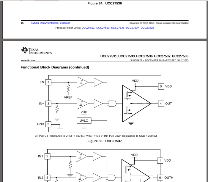
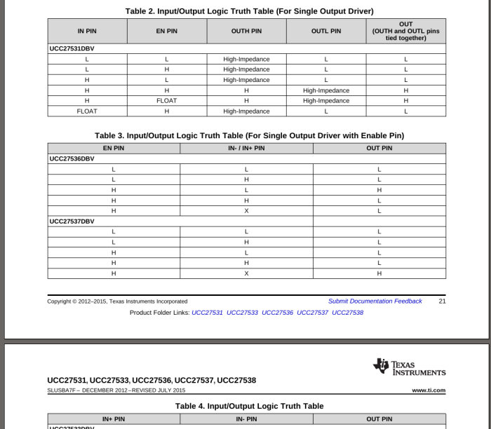
We would like to use one of the UCC27537DBV circuit. The Logic truth table for this circuit makes no sense.
Please see the picture.  UCC27537DBV circuit is a plain simple buffer and I see no meaning in that Logic truth table.
Can you please explain more about this IC?
Can I apply 30V on the VDD pin?
Can I drive this IC (pin 3 IN+) with a plain pure TTL gate at 5V?

How many IN+ or IN- can I drive with a plain pure TTL gate at 5V (output drive 24mA)?
Where is this IC enabled on High or on Low?

From the Logic truth table you (or at least I ) can not figured it out.
Thank you for your support.

Sorin Haidau

  • Hello, Sorin,

    Thanks for interesting in this part. Please see my comments:

    1. The truth table are correct. UCC27531 has two outputs. OUTH and OUTL. When IN is high, OUTH is high and OUTL high impedance if the EN is high. If EN is low, meaning IC is disabled, so OUTH is changed to high impedance, and OUTL is low. When both OUTH and OUTL are connected, OUTH/OUTL either high or low;

    2. VDD max is 35V, but IN is max 27V only;

    3. it depends on the TTL output voltage level.

    Thanks,

    Sean

  • Hello Sean,

    I meant the Logic truth table for UCC27537 not for UCC27531.
    We are interested in UCC27537.
    If I intend to drive three UCC27537 would that be enough a plain pure TTL gate at 5V (output drive 24mA)?
    Thank you for your partial answer. Part of the questions got answers.
    Thank you

    Best regards
    Sorin Haidau
  • Sorin,

    I am promising to drive three UCC without issues. The input of UCC are high impedance, and it doesn't need much current.

    Regards,
    Sean