This thread has been locked.

If you have a related question, please click the "Ask a related question" button in the top right corner. The newly created question will be automatically linked to this question.

LM74610-Q1 Load Capacitance

Other Parts Discussed in Thread: LM74610-Q1

I just came across this device, and it looks like a great fit for a reverse polarity application.  My question is about the load capacitance requirements.  If I understand the operating principles correctly, it would seem that a larger load capacitance would require a larger charge pump capacitance.  That's because the charge pump operates on the input to output voltage differential, and a large output capacitance can increase the time for this differential to build up when the MOSFET switches off.  I didn't see any recommendations or limits for load capacitance in the LM74610-Q1 data sheet, however.  Am I missing something or should the load capacitance be an issue in this design?

  • Gabor,
    Charge pump capacitor and output capacitor are two complete independent things. Charge pump operates independent of how much output capacitance is used. During the body diode forward conduction (1 to 2%) the charge pump extracts the energy from body diode voltage drop (vf) and charges up the charge pump cap (regardless of its value) through 50uA current flow. Once the charge pump cap is charged to the upper threshold value (~6.1V), this stored energy is provided to turn ON the MOSFET gate. The cap now discharges @ ~1uA current consumption rate.

    Using small or large charge pump capacitor only changes the frequency of switching between body diode and the MOSFET (Figure 8 VOUT datasheet). SO if you look at Equation 6 and 7 on the datasheet which shows a calculation of the output voltage switching frequency for a 2.2uF charge pump cap. If you use a smaller cap, the frequency will double however the duty cycle will remain the same.

    As for output cap, this device doesn't need any output capacitor to operate. However in some applications such as automotive, the battery voltage supply line can experience voltage interruptions. An output cap will keep the voltage supply to downstream electronics uninterrupted. The output cap value is up to your system requirement and has nothing to do with the charge pump operation.
    Best
    Kaisar
  • Here is a system example of LM74610 or schottky diode with small and large output cap:

    As you can see with a smaller cap, the output voltage dropped down to zero when input voltage is interrupted for 300usec. With larger cap at the output, the voltage didn't immediately drooped down to zero as a result of supply line interruption . 

  • I think we're talking about two different things here.  In your traces, the input voltage is dropping.  I was talking about the case where the input voltage is stable, but say for 300us the MOSFET is turned off for its nominal 2% duty cycle.  In the first figure, the output voltage drops quickly, and therefore the difference between Vin and Vout is soon sufficient to drive the charge pump.  In the second figure (220uF) the output voltage drops slowly, and it takes time before the MOSFET's package diode is actually conducting due to the small input to output voltage differential.  During this time the charge pump may not have enough voltage to operate.  If the LM74610-Q1 uses the gate voltage to determine when to turn the MOSFET back on, then this would increase the off time and decrease the duty cycle of the FET.  Therefore to get back to 98% on time, you'd need to slow down the charge cycle rate by increasing the charge pump capacitor.

  • Gabor, 

    It's actually very interesting question, whether having a large output capacitor will resist the sudden change in voltage (0.7 V) from MOSFET to package diode, and as a result would that effect the charge pump operation?

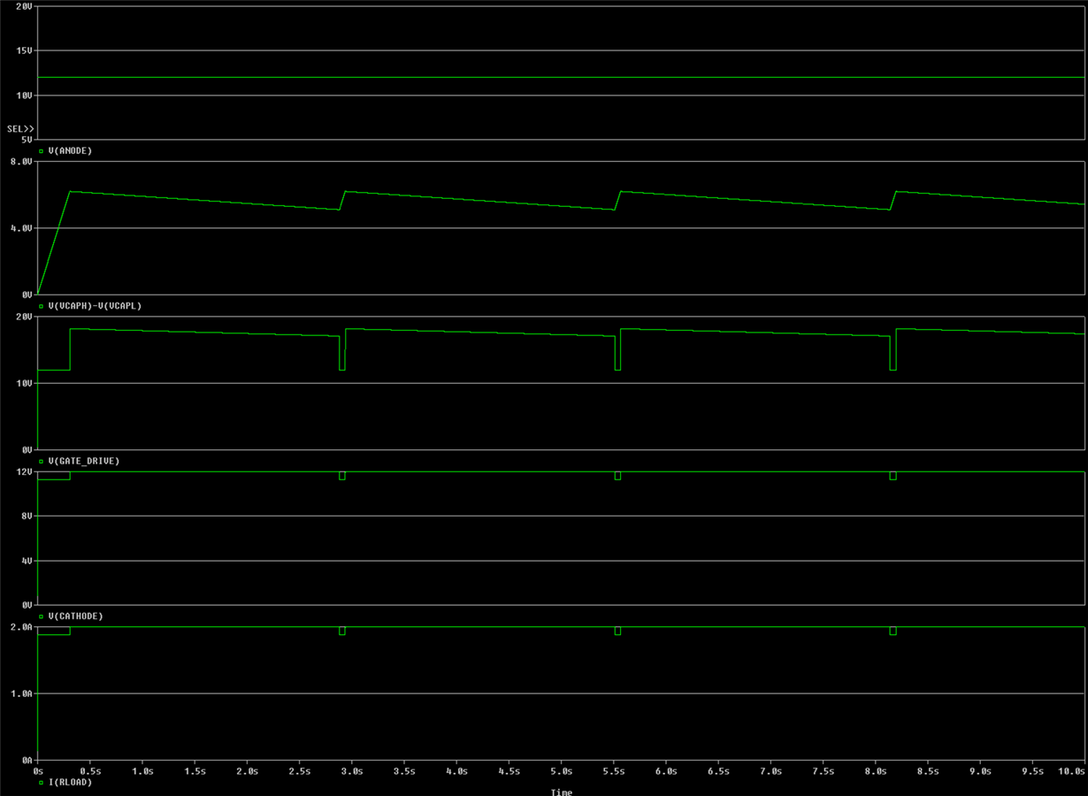
    I ran the following simulations to see whether having a large output cap makes any difference:

    In this simulation I have 12V input voltage, 2A output current (resistive load). As we can see the output voltage has body diode pulses every 2.3 sec. For the equation T = C*dV/dI, dV is change in voltage (diode drop) = 0.7V, dI is change in output current drawn = 0.1A. So we can calculate the slew rate based on the cap value ( which is 22uF for this simulation) here is whats happening: 

    So the slew rate of voltage drop from 12V to 11.3V is 0.02msec, exactly what I calculated using T = C*dV/dI. The voltage drop width time is 22msec, This is the time period when charge pump is active and charging the VCAP (change pump cap) from lower threshold (~5V) to higher threshold value (~6.1) using 50uA current flow. So If you use 2.2uF, this time will be exactly what the simulation is showing. 

    Now for comparison, I changed the output cap to 10,000uF and here is the result:

    As you can see every thing remained the same except for the slew rate for the change in voltage from 12V to 11.3V. This time it increased from 0.02msec to ~0.4msec. However, the amount of time body diode had to conduct is still 22msec. 

    So this proves a few things:

    1. Body diode pulse width doesn't depend on the output capacitor value and therefore the change pump operation is not effected by output cap 

    2. Output cap value only changes the slew rate of how fast the voltage shifts from MOSFET conduction to body diode conduction. Due to small change in voltage and current the cap value has to be unpractical and  so large to see this change. The change in duty cycle will be very insignificant. So it will remain 98%. because the pulse width increased only by 0.4msec even with such a large change in cap (22uF to 10,000uF)

    3. Body diode conduction time depends on the VCAP value only, During this time VCAP is charged form 5.1V (lower threshold) to 6.2V (higher threshold) using 50uA charging current from the change pump. 

    Hope this explanation helped, thanks for the opportunity to learn. 

  • Dear Gabor,
    Please verify if the answer is satisfactory.
    Thanks
  • OK, I see what I was missing is that this circuit is really running much more slowly than I had imagined.  So the longer slew time due to output capacitance is still small compared to the body diode conduction time.  Thanks for the clarification.