


Hello,
I made an hbridge using TPS2836 and CSD16404. The schematic is shown below. It does not work properly and I have a few questions about it. It would be great if you can point out where the design is wrong.
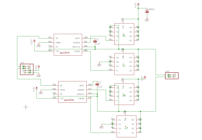
1. I gave a VDD-GND of 5V and tried to give the voltages 3.3V (signifying a logical 1) and 0V (signifying a logical 0) to the inputs of the two mosfet drivers. When I try to turn on the left-high side mosfet, the voltage at it's source is 4.5V with no load attached to the driver. The current drawn by the whole circuit is also almost 300 mA. Simultaneously, if the right bottom mosfet is turned on, the voltage at it's drain is not zero but something around 1.5V. Note that I am not giving a PWM to the inputs of the mosfet driver but direct voltage levels. Should there be a pulse train coming in to let the charge pump function properly and fully turn on the mosfet? The voltage at the gate of left-high mosfet is 5.5V which is pretty low, when the CSD16404 turns on only at VGS = 1.8V.
2. If I try to turn on the right top mosfet and the left-bottom mosfet, the whole circuit draws some 1A and things begin to heat up! It could be that the lower-right mosfet is smoked while / after soldering right?
3. Are the resistors between the mosfet driver output and the mosfet gate (not used in this circuit) essential for the functioning? They are only used to control the turn on times right?
Thanks,
Pratik C.

