This thread has been locked.

If you have a related question, please click the "Ask a related question" button in the top right corner. The newly created question will be automatically linked to this question.

TPS65185: fails to go ACTIVE - reports VCOMF

Part Number: TPS65185

Happy holidays !

Some of us need to work during Christmas and having issues with the TPS65185...

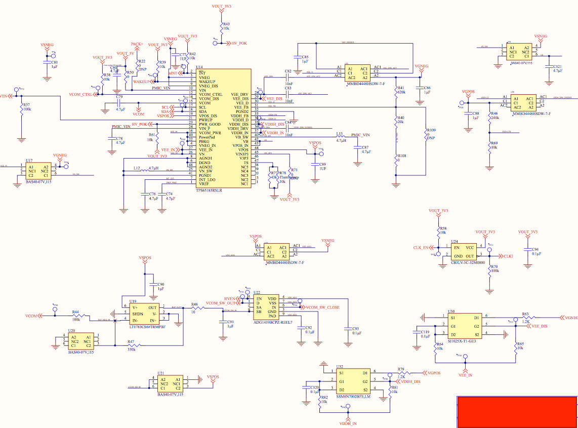
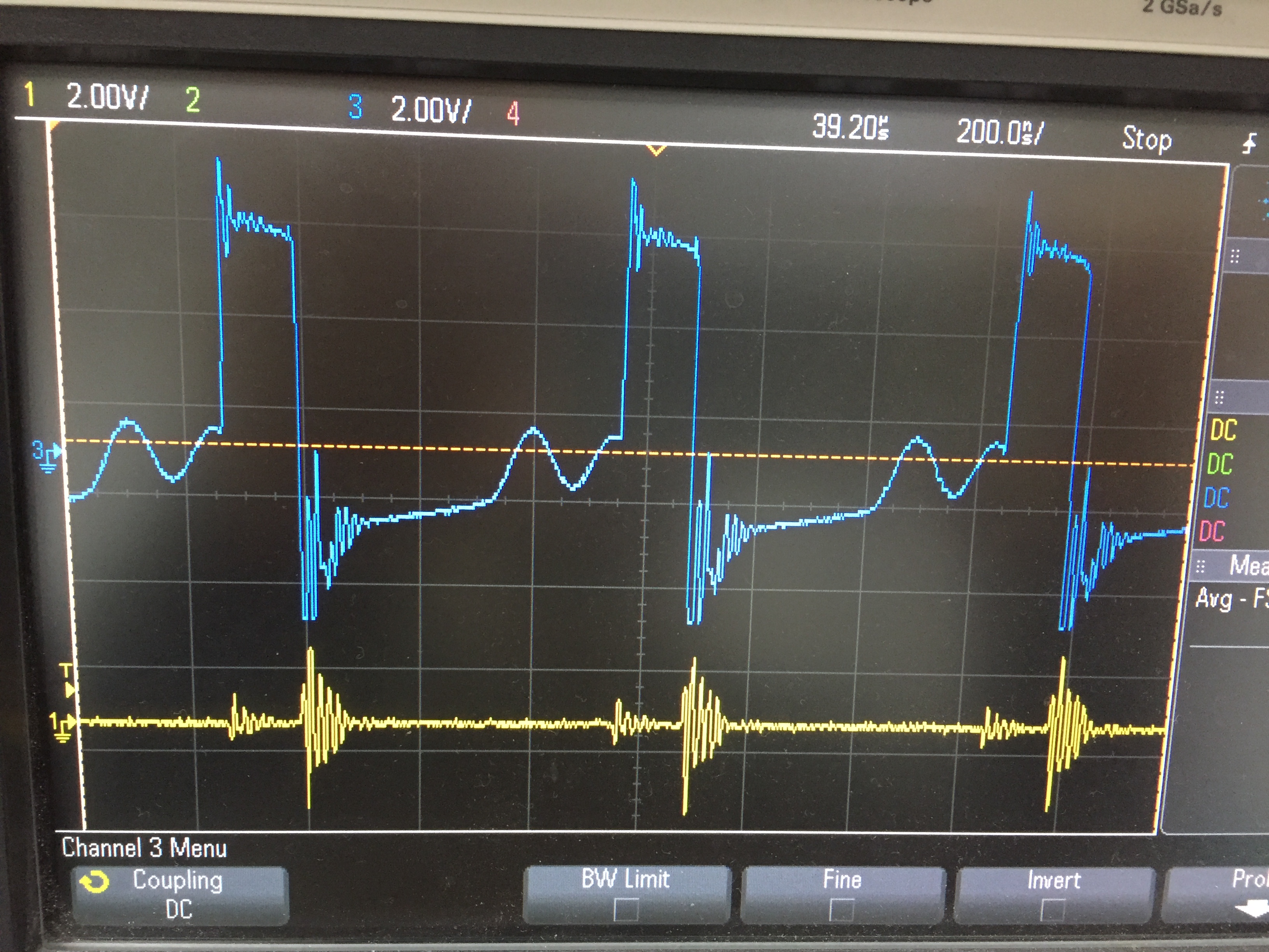
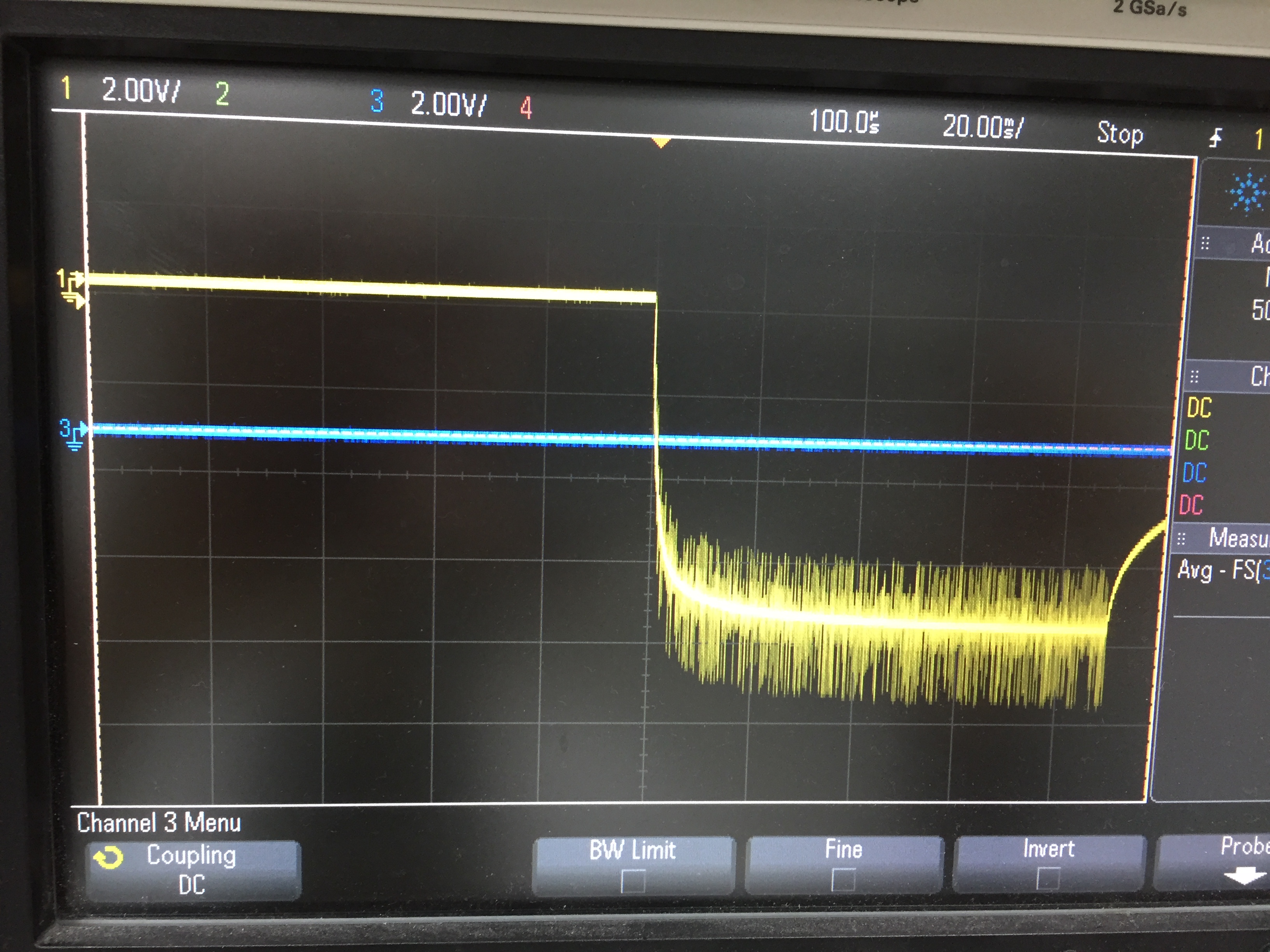
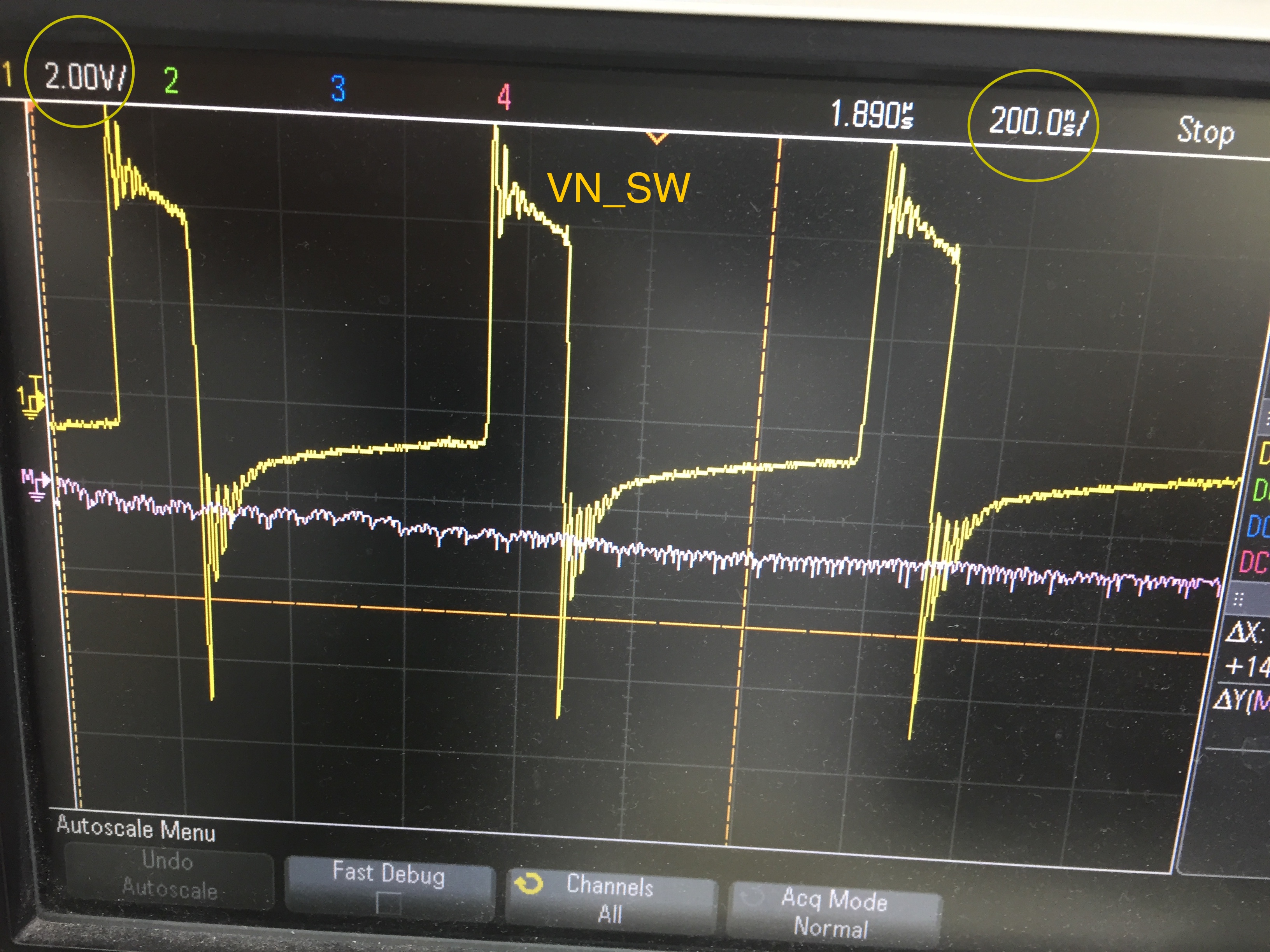
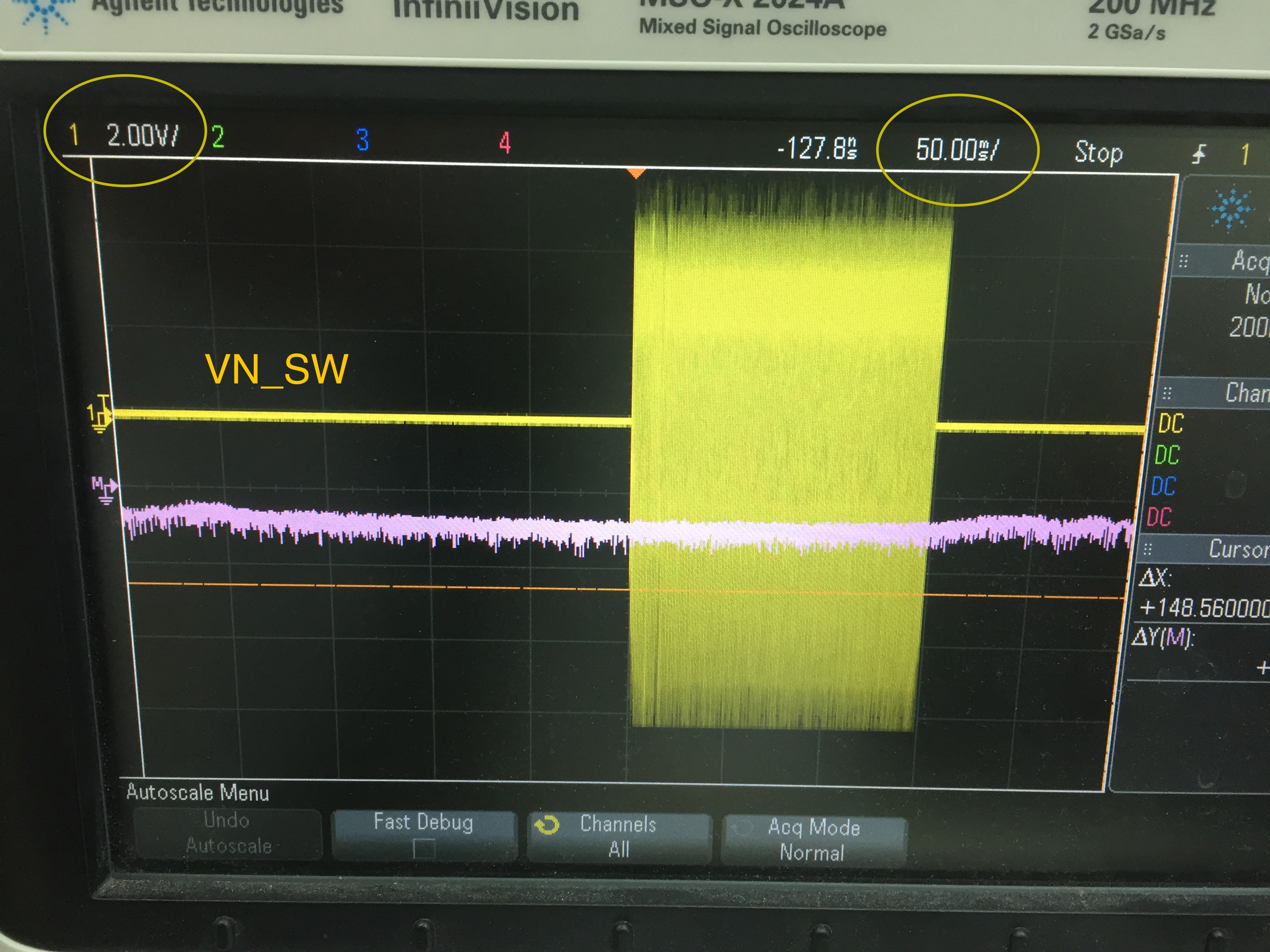
Setup is a new board, proved design and basic typical application schematics implemented.  while powering up the WAKEUP and POWERUP signals by order, the device is alive and I2C operates. But, power rails are down and VCOMF is reported via INT2 register (value is 0x04).

The issue is that VCOM_CTRL is kept LOW and while measuring VCOM it shows ~0v. VCOM1 & VCOM2 registers reflects their default value. Even setting VCOM to 0x0 does not show any change.

Also, using the I2C to POWERUP - writing 0x80 to ENABLE (0x01) register behaves the same .

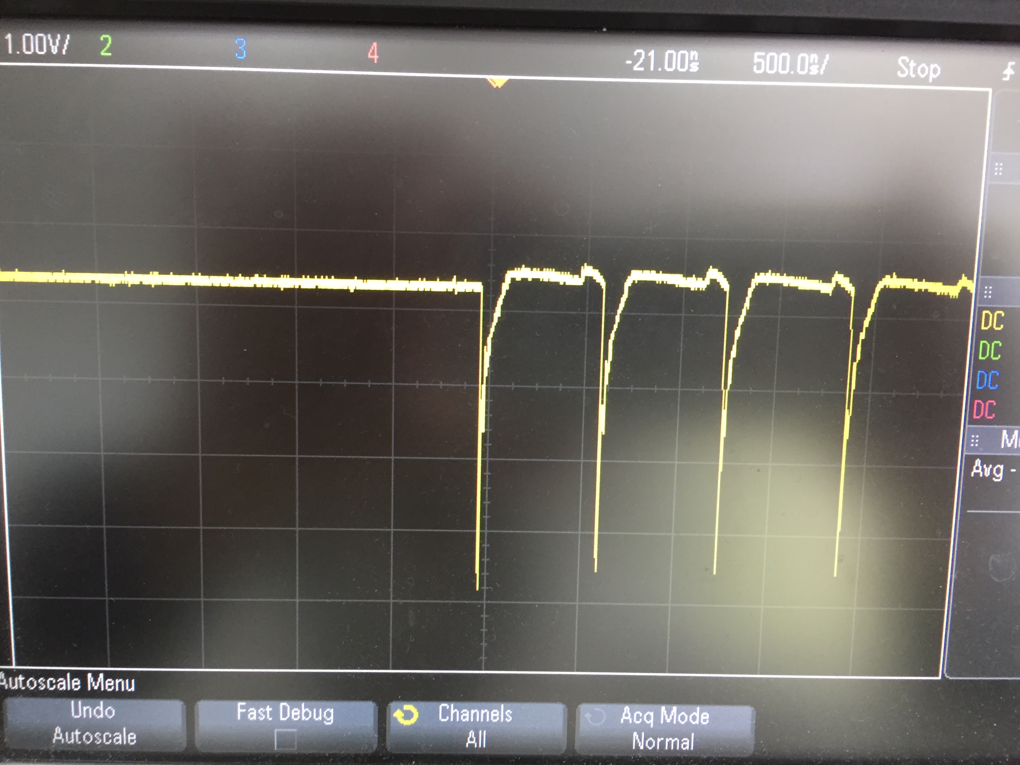
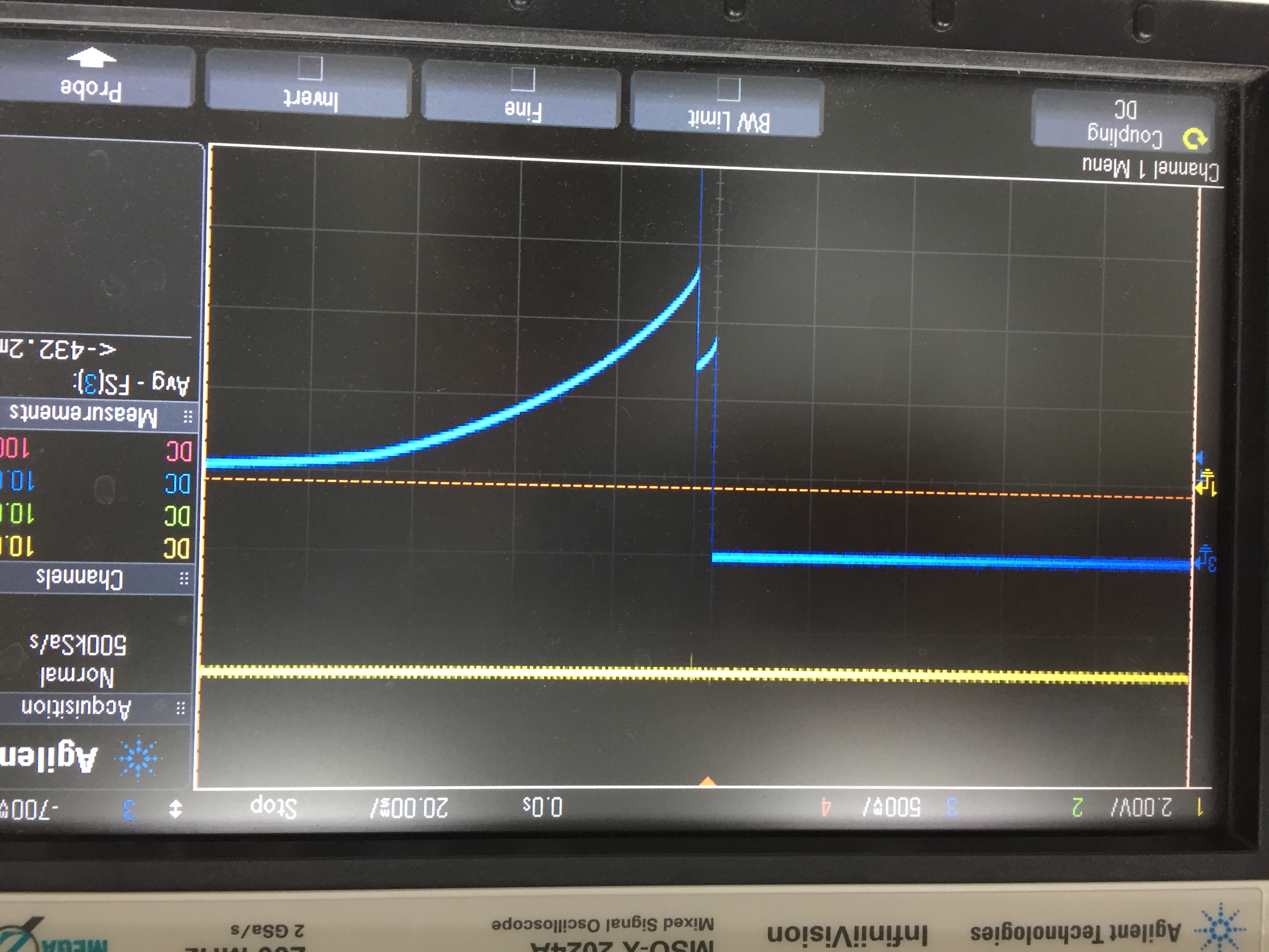
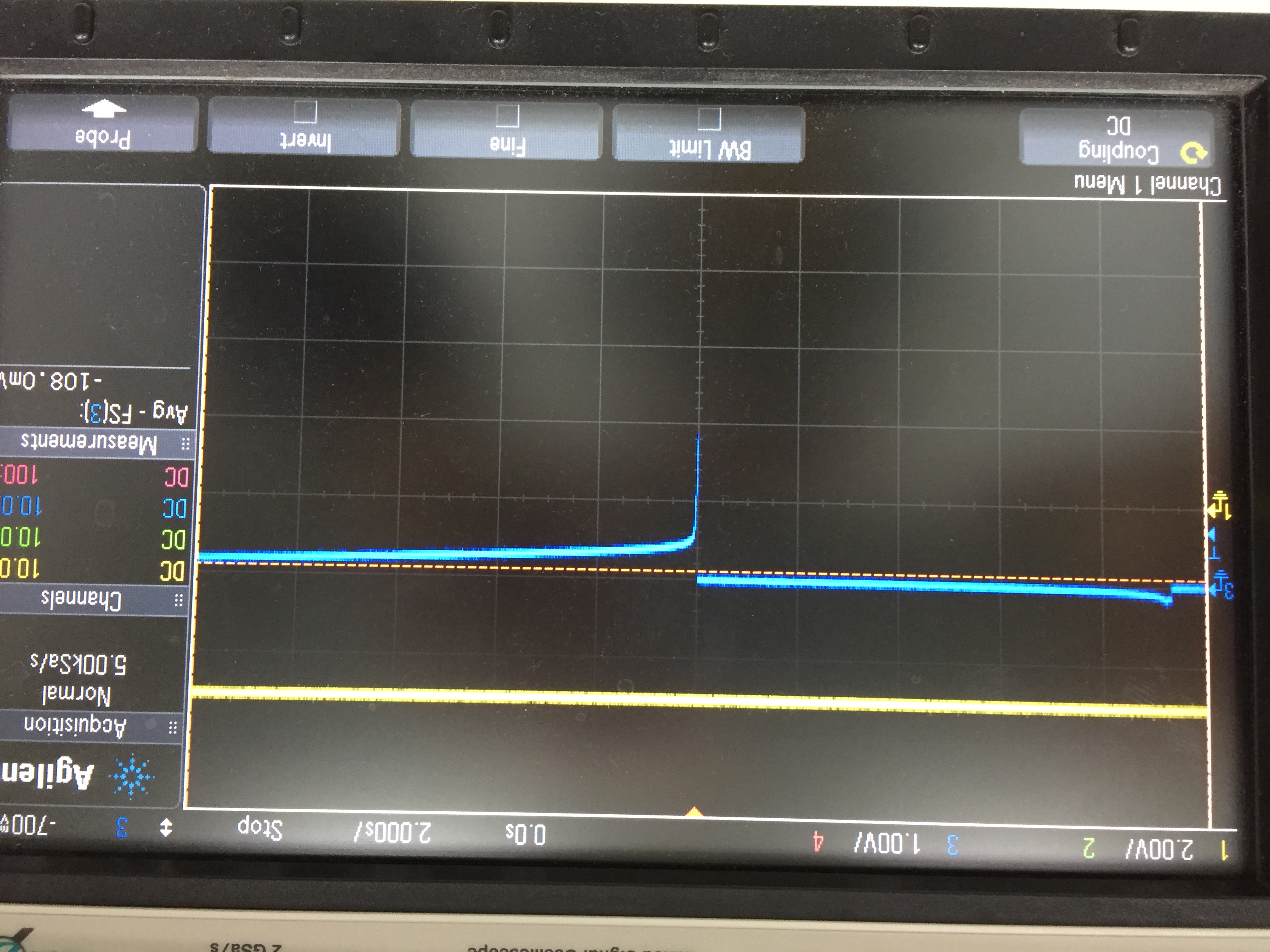
VN signal is attached. VB is constantly on 5v (=VIN) .

Any idea what might cause this?

thanks a lot for your help in advance!

Gal

  • Hi Gal,

    Are both images for VN? Could we get a closer screenshot of VN, maybe at 20mS/div? Including VIN may also be helpful.

    I would expect a VN_UV fault before VCOM_F fault.

    Can you confirm that the thermal pad is not connected to GND?

    Best Regards,
    Rick S.
  • Hi Rick, happy new year!

    Thank you for your help here.

    Double checked the thermal pad, it is connected to VN & VEE_IN (not connected to GND ). In the last post the both images where for VN .

    I would expect VN_UV fault but I never saw it, only the VCOMF for some reason.

    Please see attached new screenshots at 20msec/div. Blue = VN , YELLOW = 5v VIN:

    Any idea? 

    appretiate your help!

    Gal

  • Hi Gal,

    I can't explain this yet, how many devices have this issue? If only one, does replacing the device resolve the behavior? If this is occurring on multiple boards, would you be willing to share your schematic?

    Best Regards,
    Rick S.
  • Hi Rick,

    All of the devices tested (4) till now have this issue, even tried to manually replace the device on 2 boards, got the same result.

    in another test, I see difference in behavior in case the VCOM1 is set to 0x7D (reset value) or 0x10 (see below). Seems that the VN is not generated so the VCOM generates positive voltage and hence VCON fault, make sense?

    In addition, please examine the schematics . pls note these small fixes already implemented : R45 is removed, VB connected to VDDH_IN, added 10uF cap from VN to gnd.

    appretiate your support!

    looking forward for any ideas.

    Thanks

    Gal

  • Hi Gal,

    Yes there seems to be a relation between VN and VCOM, and a single 10uF on VEE_IN may not be enough to resolve the issue. Placement of the cap should also make a difference, where it would be best to bridge A1 on U17 directly to the ground pin of L12, and even still the external capacitor may not be enough depending on the layout of the board. It is also recommended to have a small dedicated capacitor for VCOM_IN. A scope shot comparing VN_SW and VCOM on a smaller time scale may help with debugging this behavior.


    Best Regards,
    Rick S.
  •  Hi Rick,

    Pls see below the scope shots , VN_SW in Blue, VCOM in Yellow.

    This is another device with closer caps.

    Thoughts?

    Thanks

  • Hi Rick,

    After placing additional cap on A1 of U17, as you've suggested, I see improvement of the VN signal, and now it drops to -8v and VN_UV is generated.

    VN is in yellow.

    What might cause VN not to be able to reach its -16v?

    Thanks for your help so far!

    Gal

  • Hi Gal,

    Is the VCOM_F interrupt still occurring?

    It looks like the noise on the VCOM rail was coupling to the probe, thank you for the closer scope shots.

    Anode to the inductor is the best placement for the output capacitor, but now what is the total output capacitance on the boost? There is a ~50mS deglitch on VN_UV, and decreasing output capacitance can reduce the time it takes to reach the regulation target. It may also help to investigate the input capacitor as well. Replacing C78 with 10uF and trying to connect VIN_P directly to the common ground pin on the inductor may also help. Probing this rail will show if the input voltage is decreasing as the output capacitors charge eventually as the other regulators are enabled.


    Best Regards,
    Rick S.
  • Hi Rick,

    No, the VCOM_F does not occur anymore. Now the VN_UV is constantly occurring.

    You can see below the signals of VN_SW and VN:

    I've tried to increase the cap of C78 to 10uF and reduce it, no change.

    The VIN is extremely stable, injected from external power supply @ 5v with practically no current limit.

    Any idea how to proceed ? 

    Thank you!

    Gal

  • Hi Gal,

    Can you confirm the current rating of your rectifying diode? From the schematic it looks like it could be 150mA, but the switching current limit of VN is typically 1.5A. Our EVMs implement 1A average rated diodes capable of 5A peak

    I do not see a clear low side in the switching cycle, and if the diodes cannot handle the switching currents it could explain this behavior.

    Best Regards,

    Rick S.

  • Hi Rick,

    First, I want to thank you for your support till now!

    Second, we're making progress here as I took your advice and replaced the U17 diode with Schottky diode (2A, 30v) and also replaced L12 inductor to 4.7uH 1.9A/90mOhm, VN capacitor is 4.7uF / 50v. The result looked promising, now I see VN drops very fast to -30v (I expect it to get to -16v) and no error is generated via INT1/INT2!! clearly VB and other rails are not generated.

    Please see image of VN:

    Any idea what might cause VN to overshoot like that?

    seems that the DCDC2 supposed to work independently of other passive components connected to the PMIC, correct?

    thanks again,

    Gal

  • Hi Gal,

    DCDC2 can work independently, but this could happen if the feedback pin (VN) is not actually connected to the output capacitor, as it uses this node to regulate the target voltage and recognize UV/OV conditions. Is there any chance the new components are not connected to VN?

    Best Regards,

    Rick S.

  • Hi Rick,

    I see your point, but the VN capacitor is well connected. I've double checked and even added more capacitance (4.7uF vs ~14uF) and saw VN rise/fall time becoming longer respectively.

    I've captured the VN_SW herein (both images) and it looks strange:

    Thoughts?

    Thanks,

    Gal

  • If these voltages were confirmed at the VEE_IN test point, the VN pin (26) might be damaged and the part may need to be replaced.

    Best Regards,

    Rick S.

  • Hi Gal,

    Did this resolve the issue?

    Best Regards,

    Rick S.

  • Hi Rick,

    Thank you for the follow up.

    No, I'm afraid we're stuck. tried to replace the part but the manual replacement wasn't successful.

    I have tried to build a new test setup trying to isolate the DCDC2, I've connected  VIN/VIN_P/WAKEUP/PWRUP to their signals and connecting VN/VN_SW to the relevant L/diode/cap, but the device didn't generate any voltage on VN . (powering up sequence was performed manually).

    next we'l manually fix another board. 

    Pls let me know if you have other direction/idea . 

    Best regards,

    Gal

  • Hi Gal,

    While DCDC2 is the first regulator in the sequence and will boot independently, after it successfully regulates an undervoltage fault on VB will also shut the device down. However it does not seem that we are getting to this stage if no voltage at all is appearing on VN.

    Please also ensure the power-pad (PBKG) is connected to VN.

    Best Regards,

    Rick S.