This thread has been locked.

If you have a related question, please click the "Ask a related question" button in the top right corner. The newly created question will be automatically linked to this question.

LM2596: Catch diode failure

Part Number: LM2596

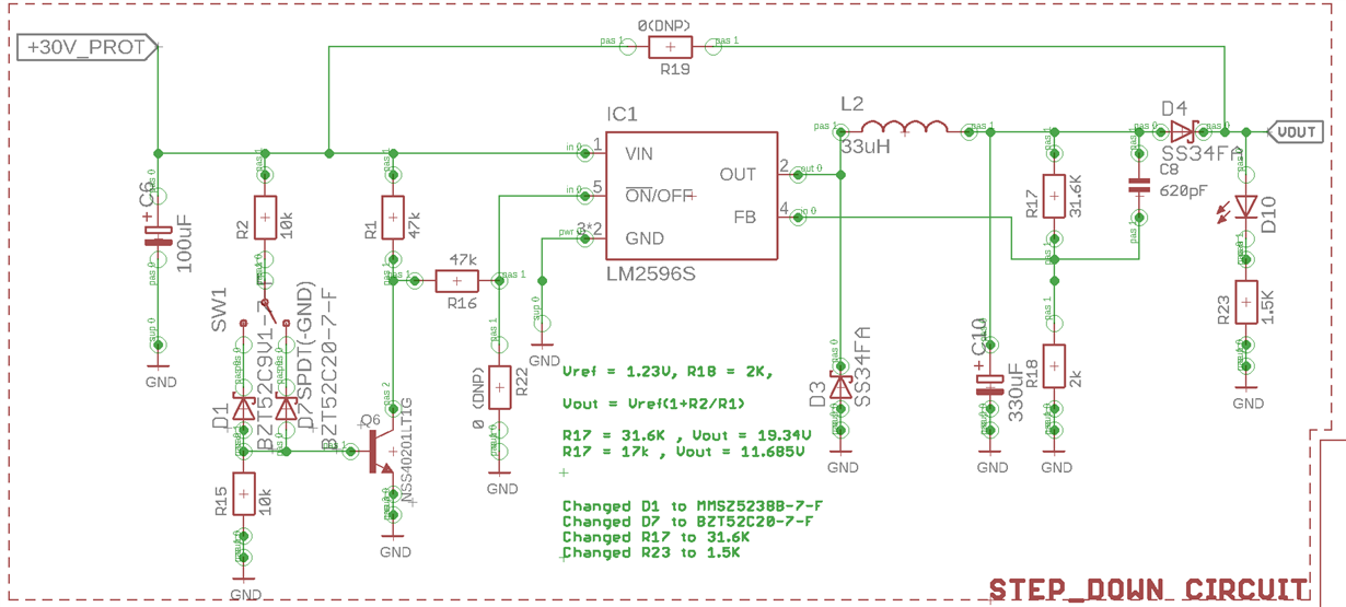
We are using the LM2596S-ADJ to buck from around 28V to 20V drawing about 1.8A at the input to the circuit.

(The schematic is below.)

We have seen a number of instances where the catch diode D3 (SS34FA) fails.  We suspect that the RMS Reverse Voltage of the SS34FA may be insufficient and have upgraded to the SS36FA but we have been unable to make either fail in the lab and would like to verify before re-deploying to the field.

The circuit is used in a vehicle application and is preceded by a 24V version of SNVA717 for protection which seems to work fine.

Any ideas what we may be doing wrong?

Thanks


  • Hello,

    At first look the original diode is rated to 40V which is greater than 1.25 times of 30V maximum input. Also, the reverse recovery time looks good. The most stressful condition will be heavy load or short circuit condition. The diode should be rated to 1.3 times the maximum load.

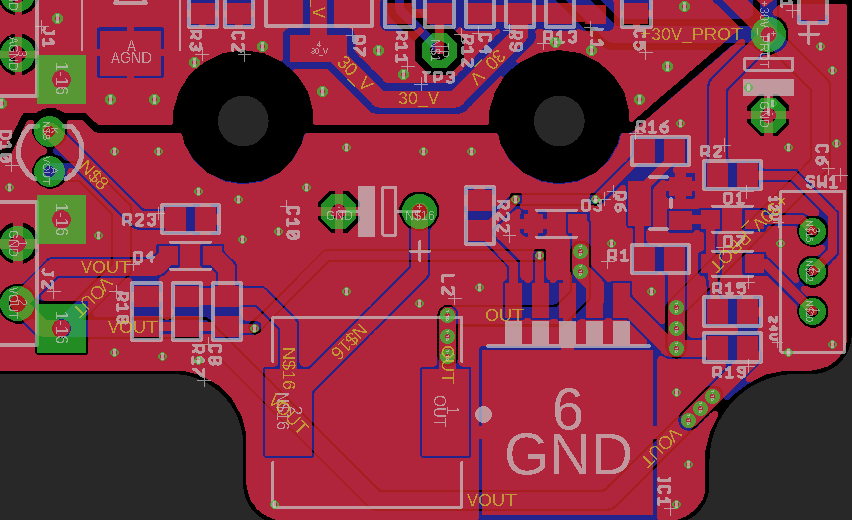
    Under what conditions does the catch diode fail - start up, transient conditions, steady state? Could you also share the layout for this design?

    Thank you,
    Katelyn Wiggenhorn
  • Hi Katelyn,

      Thanks for the quick response!

    I took some time to pull up the layout and review it.  I do see a number of things that aren't ideal but I'll let you comment (wish I had caught them during review!)

    We find the failures after a few days in the field so assuming it is during steady state during heavy load.  (It does not fail during startup and the automotive protection circuit cleans up any transients.)

    Thanks,

    Kurt

  • Hello Kurt,

    What is the typical load conditions for this application? One possibility is that you need to use a catch diode with a higher current rating.

    Second, the datasheet recommends using a heat sync on this device. Does your board use a heat sync? How many layers are there? Does this design use internal layers to dissipate heat from IC? Looking at your board, this device could be operating very hot for an extended period of time. The maximum operating temperature of the diode is 125C while the maximum temperature of the IC Is 150C.

    For the schematic, my recommendations are:

    1. R18 is recommended to be between 240Ohm and 1.5kOhm. Then calculate R19 accordingly. This is to minimize the nose of the sensitive feedback pin. The feedback resistors should also be as close as possible to the feedback pin.
    2. What is the ESR of C6? A low ESR aluminum or tantalum cap is required close to the input of the device.

    For the layout, my recommendations are:
    1. SW node is routed on the bottom layer under the device and under the FB pin. This trace and FB should be routed away from each other. I would recommend keeping the SW trace on the same layer and using a larger trace to connect the two.
    2. I would recommend keeping a solid input plane to the device. I am unclear on the location of C6, but it is further away from the device than recommended.

    Please use the EVM as an example layout, and please let me know if you have any questions.

    Best Regards,
    Katelyn Wiggenhorn
  • Hi Katelyn,

      The max load is 1.8A and this lasts a couple of hours until the battery is charged up.  Please clarify if you feel the current rating of the SS34FA or SS36FA (3A) is too low.

      Unfortunately we do NOT use a heat sink on this device.  This is a two layer board with 2oz copper pour.  However the board is fairly compact so there is little room for heat dissipation.  

      Thank you for noticing R18, I will definitely have that updated.

      C6 is an aluminum cap (UVK2A101MPD) from Nichicon, the ESR is not listed in the datasheet.

      Yes, the routing comments you mention are well noted.  I wish I had seen that earlier when I was reviewing the board.

    Thanks,

    Kurt

  • I think that C6 is too far from the IC. Also, you may need a small 0.1uF or 1uF near the IC.
    It could be that you are getting spikes at the SW pin that could damage the diode.
    Can you get a 'scope shot of the SW pin ?
  • Hi Kurt,

    The diode's current rating of 3A is greater than 1.3x the load current. This should be sufficient.

    Best Regards,
    Katelyn
  • Thanks all,

      I will redo the layout with those points in mind.

      I'm working on getting the SW pin scoped - (Just out of office so have asked a co-worker to look into it)