This thread has been locked.

If you have a related question, please click the "Ask a related question" button in the top right corner. The newly created question will be automatically linked to this question.

TPS7A49: TPS7A49 TPS7A4901 regulator output voltage error / creeps up

Part Number: TPS7A49

We have a design which contains a 3 rails regulated using the TPS7A4901DRB.

The input voltage is between 6 and 12 V.

The output voltages are 5.0V, 3.3V, 2.5V.

The output load on these rails is a few mA (<10mA).

We have observed on some units that the output voltage creeps up, but this can take a few hours to manifest.

Some show the 5V floating up to 6V and others the 3.3V floating up to 4.0V. 

This problem is more prevalent when the input voltage is 12V.

As an experiment we increased the input to 15V and saw a dramatic reduction in the time required to observe a fault.

We also noticed that if a reduced voltage is presented on the Enable pin (originally tied to Vin, 12V) then the fault is much less likely to manifest.

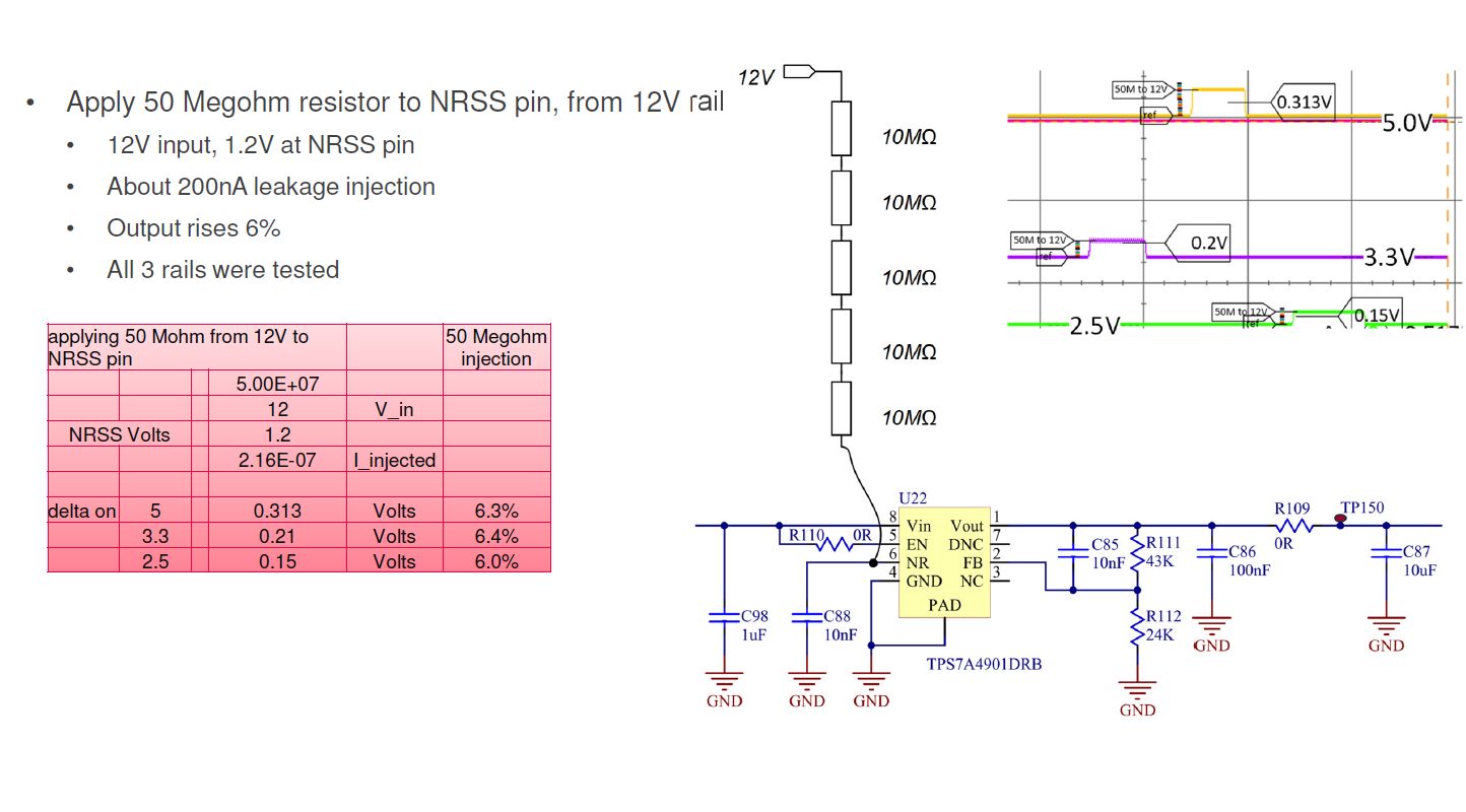
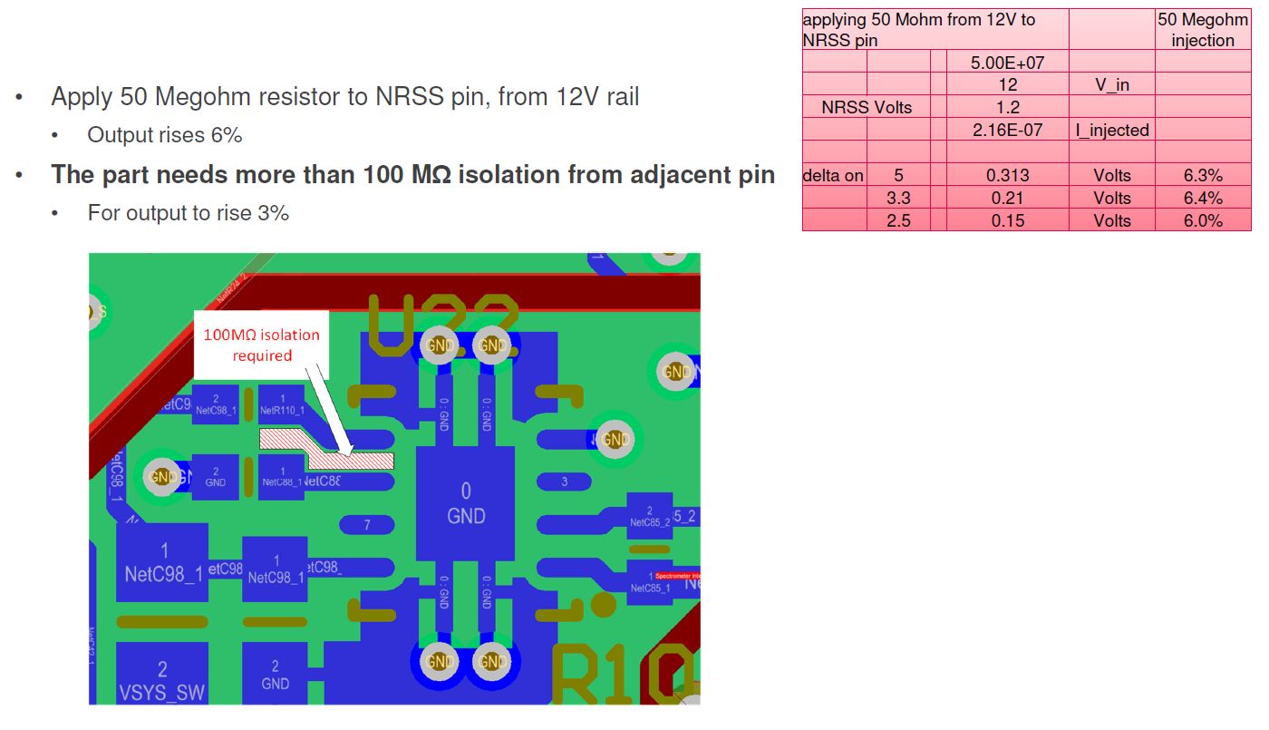
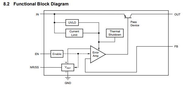
We noted a previous Ti forum thread, which mentioned a very high input impedance on this pin, and the EN pin is very close to the NR pin. Therefore as an experiment we investigated what isolation is required between the NR and EN pins by connecting the same input voltage onto the NR pin through a series of resistors as shown in the image below.

Even with a 50Meg ohm series resistance, distortion of the output voltage by 6% was observed. This implies that over 100Meg of isolation is required between these pins for correct operation.

Please could you confirm that this level of isolation is reuiqred between these pins for correct operation.

  • Hi Mark,

    The NR pin allows for an external capacitor to be used to filter the internal reference of the TPS7A49.  Since the output voltage is a gained version of the reference, the NR pin should ideally be completely isolated from any other voltage rail.  

    Often when the LDO output is not the set value it is due to an unintentional bias.  Sometimes this bias can come in the form of residual flux from the assembly process.  From your investigation it looks like you are suspecting an unintentional leakage path between EN and NR.

    Very Respectfully,

    Ryan

  • Hi Ryan,

    Thank you for the quick response.

    Correct we are indeed suspecting contamination or a leakage path between these pins.

    But what surprises me is how sensitive the NR pin is to such contamination.

    Our experimentation suggest that 100Meg across the 0.35mm gap between the EN and NR pads ,when run from a 12V input on EN would be enough to cause a 3% error in the output.This required impedance would be significantly less at input voltages approacing the higher end operating input of 36V

    Also at this level of impedance even blowing on a device would cause distortion on the output of the device - which indeed it does!!

    Is it really this sensitive? In which case is it suitable to use the VSON package at higher input voltages?

    Please advise.

    Mark.

  • Hi Ryan, Thanks you for your response. Did you see my further comments below?
    Mark.
  • Hi Mark,

    I apologize for the delay. We do expect a large amount of impedance between NR and any voltage rail including GND. As shown in the block diagram, the NR pin is connected to the internal reference. Since the output voltage is equal to the reference gained by the feedback resistors, any bias that leaks onto the NR pin will impact the output voltage.

    It is suitable to use the VSON package at higher input voltages; however, you should be sure to remove any residual flux after soldering. Flux that is not properly removed after soldering can provide an unintentional leakage path allowing the NR pin to be biased.

    Very Respectfully,
    Ryan