This thread has been locked.

If you have a related question, please click the "Ask a related question" button in the top right corner. The newly created question will be automatically linked to this question.

LMG1020: How to improve the rising and falling edge waveforms

Part Number: LMG1020

Hello!

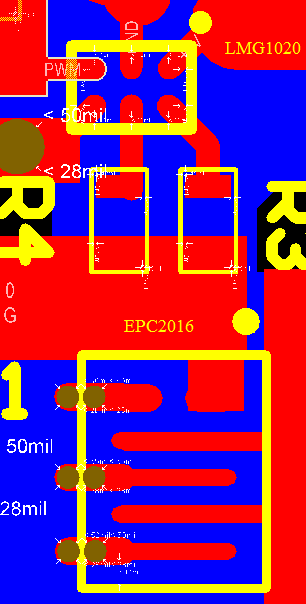
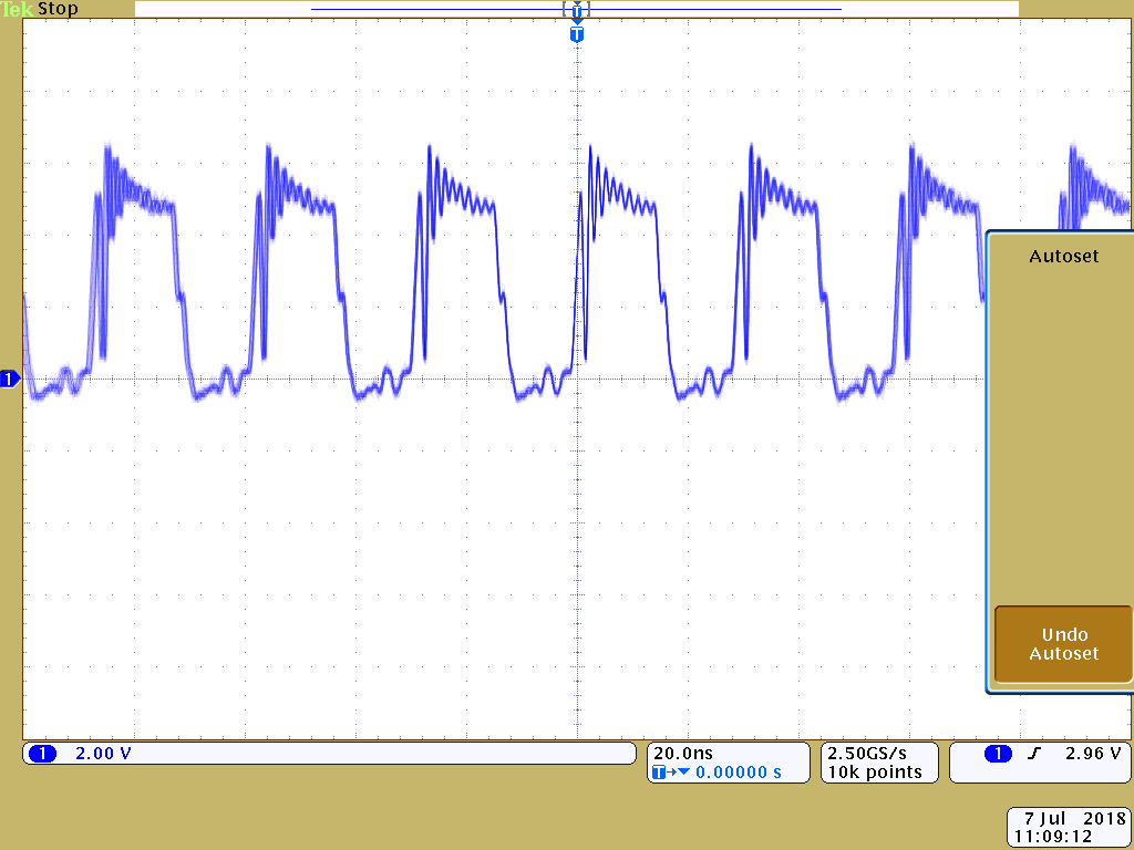
I use LMG1020 to design boost circuit. The Miller effect on the rising edge is very prominent. Can you give me some advice on how to improve the rising and falling edge waveform?  The figures below show the layout and waveform of my circuit. The input signal is a square wave of 50% .

Looking forward to your reply. Thank you!

  • Hi user,

    Welcome to e2e! thanks for asking about LMG1020. Im an apps eng and will help out.
    The miller region is defeated with high peak current or finding a way not to switch the FET as hard with less Vds Ids overlap. if SW slews too fast this can cause Cgd to be larger.
    Can you share the portion of the schematic as well with me? what fet is used?
    is the waveform of the driver IC output pins or the fet gate source pins?

    Thanks,
  • Hello,

    Besides what Jeff has mentioned, here are some other tips:

    1. Please make sure that you have the optimal layout. It can be seen from the screenshot that your gate is still some distance away from the driver, and your decoupling cap is not closet to the driver pin too. Please refer to our reference design and layout guide in the datasheet to achieve the most stringent layout.

    2. For measurement, please refer to our EVM user guide for the best way to signal probing. Please make sure that you have no ground clip, which can result in severe ringing in the waveform. Use pigtail test point please. A lot times, the waveform noise is from measurement.

    3. I see that you are using EPC2016. GaN FETs usually have very small Cgd which means very short miller plateau. In addition, our driver is very high on current capability. Therefore, you should not see too much miller region.

    Hope it helps.

    Thanks and regards,
    Lixing
  • The FET I use is EPC2016C.
    The waveform I showed is of the fet gate source pins.
  • Thank you for your reply. I will try to optimize the pcb layout.
    There is another question. The drive resistance R3=R4=2ohms in my circuit. Can I change the 2 ohm resistance to 0 ohms to shorten the miller plateau.
  • What's more, the drive IC is very hot after working for a while, and then the whole board became hot. I am not sure whether the drive IC can work for a long time. Do you have any advice on heat dissipation of this drive IC?
  • Hi user,

    Thanks for the update and Thanks Lixing for helping out!

    Its possible that the driver is still performing and the oscillations on the gate are not seen on the driver pin. Besides trace inductance adding to the voltage swing on the switch node, we need to limit the slew rate of Vds because a current equal to Cgd * dVgd/dt is flowing into the gate due to the miller effect and if the drain voltage swings too fast there will be a large current seen at the gate. Therefore we need to reduce the turn on time by increasing the turn on resistor a few ohms. Check out this app note to help with this gate resistor selection (www.tij.co.jp/.../slla385.pdf)

    Let me know if you have any more questions.
    Thanks,
  • 1. You can change R3 and R4 to be 0Ohm. But please also be aware of the overshoot caused by parasitic and you won't have too much resistive damping.

    2. The temperature rise of LMG1020 depends on your frequency. This IC have been tested for typical value at 30MHz with 100pF load, and we have not seen significant temperature increase.

    Thanks and regards,
    Lixing
  • Thank you for your kind reply!
  • OK. Thank you for your kind reply!