This thread has been locked.

If you have a related question, please click the "Ask a related question" button in the top right corner. The newly created question will be automatically linked to this question.

Flyback reflected voltage

Other Parts Discussed in Thread: UCC28610, UCC28600, UCC24610

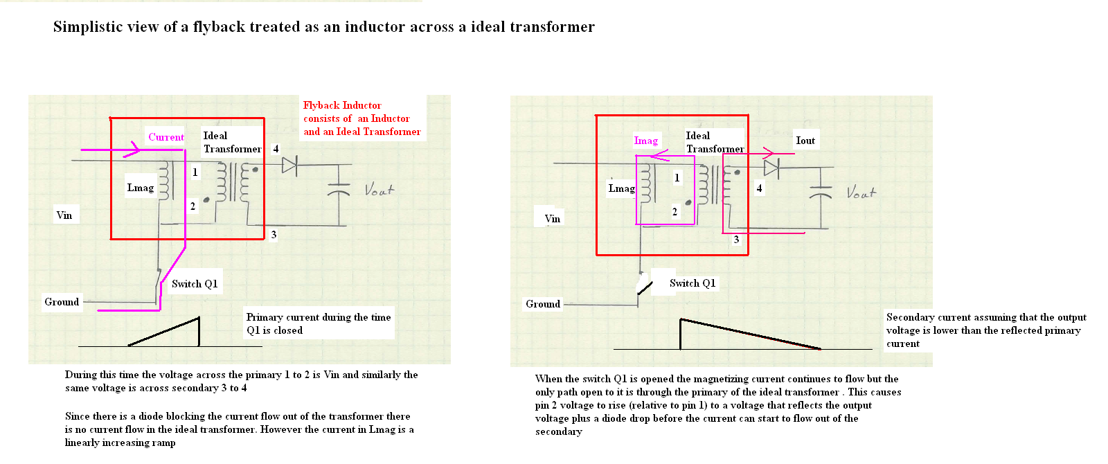
I am trying to understand when exactly the voltage is reflected from secondary back to the primary.
 
1. The primary Switch turns ON, the primary inductor current ramps up
2. The primary switch turns OFF, current is induced in the secondary inductor-->diode conducts -->capacitor charges
3. The capacitor is charged to Vo and diode acts like open switch. The secondary inductor discharge is cut off because of this.
4. The primary switch turns ON again and the secondary voltage is reflected to the primary side???
 
Is my understanding correct ?
Can I see this action in ckt sim like LTspice.
 

  • Please refer to the scope image enclosed.  This image shows the switching of the UCC28610, a discontinuous flyback controller.

    The Gate signal turns off the primatry switch after the current in the drain ramps up (IDRV on Ch 1).  The drain on the primary switch will notw increase to the sum of the input voltage nad the reflected output voltage until the transformer has demagnetized .  After the transformer demagnetizes, the primary side drain will resonate due to device parasitics with an average value of the bulk input voltage (this is the dead time)

    Flyback drain.pdf
  • should have spell checked...so sorry:

    The Gate signal turns off the primary switch after the current in the drain ramps up (IDRV on Ch 1).  The drain on the primary switch will now increase to the sum of the input voltage and the reflected output voltage until the transformer has demagnetized .  After the transformer demagnetizes, the primary side drain will resonate due to device parasitics with an average value of the bulk input voltage (this is the dead time).  Note there is also the added voltage spike on the drain at the moment the GATE signal turns off due to the leakage inductance of the transformer and the output capacitance of the primary side switch.


  • Lisa Dinwoodie said:

    should have spell checked...so sorry:

    The Gate signal turns off the primary switch after the current in the drain ramps up (IDRV on Ch 1).  The drain on the primary switch will now increase to the sum of the input voltage and the reflected output voltage until the transformer has demagnetized .  After the transformer demagnetizes, the primary side drain will resonate due to device parasitics with an average value of the bulk input voltage (this is the dead time).  Note there is also the added voltage spike on the drain at the moment the GATE signal turns off due to the leakage inductance of the transformer and the output capacitance of the primary side switch.


    So, the moment the primary switch goes off, secondary diode starts conducting and simultaneously secondary voltage is reflected on to the primary coil?

    I was thinking, since the secondary side is not conducting when the primary switch is ON, there's no mag field in the coil. So no energy stored. But when the switch goes OFF, where does the secondary get it's energy from?


  • A flyback transformer is actually more accuratlely a flyback inductor... the main purpose of the flyback inductor is to store energy and then transfers it. 

    When the gate signal turns the primary side switch on, current starts to flow in the primary side windings, the magnetic flux in the transformer increases.  A voltage will be induced across the secondary side windings with a polarity that reverse biases the secondary side diode (note the dot notation on flyback transformers).  As soon as the primary side FET turns off, the energy that is stored in the transformer is equal to 1/2*L*Ipeak^2.  The transformer needs to maintain the magnetic flux and the only way it can do this is to reverse the voltage across the secondary windings so that will forward bias the secondary side diode.  The energy that was stored in the flyback inductor is dumped into the load and charges the output capacitor, the current in the secondary diode ramps down to zero when all of the energy is transfered.

  • Lisa Dinwoodie said:

    A flyback transformer is actually more accuratlely a flyback inductor... the main purpose of the flyback inductor is to store energy and then transfers it. 

    When the gate signal turns the primary side switch on, current starts to flow in the primary side windings, the magnetic flux in the transformer increases.  A voltage will be induced across the secondary side windings with a polarity that reverse biases the secondary side diode (note the dot notation on flyback transformers).  As soon as the primary side FET turns off, the energy that is stored in the transformer is equal to 1/2*L*Ipeak^2.  The transformer needs to maintain the magnetic flux and the only way it can do this is to reverse the voltage across the secondary windings so that will forward bias the secondary side diode.  The energy that was stored in the flyback inductor is dumped into the load and charges the output capacitor, the current in the secondary diode ramps down to zero when all of the energy is transfered.

    I understand this part. 

    But I still don't understand why the secondary voltage gets reflected when the switch turns OFF. 

    Secondary has some voltage built up during primary current ramp up. Correct?

    when switch is turned off, the secondary voltage is reflected onto the primary side and at the same time, voltage across secondary windings is reversed, and diode is fwd biased?


  • Hithesh,

    See  the attached diagram for an explanation.

    Regards,


  • Dear Lisa,

    I am designing the flyback adaptor with UCC28600. Some parameters: Vin_min = 80VDC, D_max = 0.47, Vo' = Vout + Vf = 19 + 1 = 20VDC.

    But i wonder how to right calculate n = Npri/Nsec.

    Following slup127.pdf TI's document, n = Vin_min/Vo'*D_max/(1 - D_max) = 3.54

    Following SLVC104I.xls, n = 7.2 is recommended and n = Vxfmr/Vo' and Vxfmr = 142V is recommended

    So could you help me to understand what is Vxfmr and how to calculate it? Vxfmr = Vin_min + n*Vo' is it true?

    Which document can i use to calculate the turns ratio of transformer, n?

    Thank you,

    Son.

  • The turns ratio is based upon 1) how much voltage can be placed  upon the MOSFET switch, OR 2) How much blocking voltage is required for the secondary side diode, OR  3) is there a duty cycle limitation that must be met?

    1)  So one approach is to calculate the turns ratio of Npri/Nsec (Nps) is to limit the voltage on the MOSFET to be equal to some de-rated value of the maximum drain to source voltage:

    Nps = Vds(max allowed) / (Vout+Vf)

    The reflected voltage, also referred to as the Flyback voltage, from the secondary is added to the maximum rectified input voltage, the voltage spike resulting from leakage inductance and parasitic capacitance is also added to this and the entire sum should not exceed the Vds rating of the MOSFET switch and there should be enough margin to account for de-rating. This is a very common approach to determining Nps and this is what is used in SLVC104, where Vxfmr is the allowable reflected voltage and leakage spike that will not exceed the desired d-rated voltage on the MOSFET switch.

    2) Or you may need to design around the limitations of the blocking voltage of the secondary side rectifier (for instance if you were using the UCC24610 synchronous rectifier controller on the secondary side you must limit the blocking voltage to less than 50V so this will dominate the turns ratio consideration):

    Nps = Vbulk(max) / [Vd(blocking)-Vout]

    and then calculate the maximum voltage stress that will be on the primary side MOSFET and select the MOSFET accordingly...the lower the blocking voltage on the secondary side the higher the voltage stress on the primary side.

    3) OR  the controller may have maximum duty cycle limitations at which point the turns ratio need to consider the energy transfer at the minimum bulk input voltage (as determined by the input ripple on the input bulk capacitor so keep this in mind...it is at the valley of the input ripple voltage that you need to calculate this) at maximum load and then the turns ratio is calculated by the equation shown in SLUP127, then the MOSFET and diode are selected based upon the resultant flyback voltage of Nps*(Vout + Vf)


    Any of these approaches will give you a turns ratio that is suitable for your design requirements but the first question is what are your design constraints?  Are you limited by the MOSFET Vds, the blocking voltage on the secondary side, or the duty cycle of the controller?  Each of these concerns may result in a different calculated turns ratio.  The rest of the power stage design will calculate the required primary inductance, peak primary current, switching frequency, etc. to satisfy the energy transfer for the design based upon the turns ratio selected.

  • Thank you very much, Lisa

  • Hi all,
    I am working on flyback first time and i am facing problem in deciding transformer for 0.5A/5V. please help me!!!!