This thread has been locked.

If you have a related question, please click the "Ask a related question" button in the top right corner. The newly created question will be automatically linked to this question.

UCC28950 / abnormal gate function

Guru 29690 points
Other Parts Discussed in Thread: UCC28950, UCC3895

Hi,

I’d like to ask about the function of UCC28950.

My customer evaluates load transient on his DCDC converter board, but he found some abnormal function.

He confirmed that outC/D lock up for 1 cycle after load transient(500mA→50A) regardless of outA /B waveform is normal, and he said this causes bias magnetism of transformer.
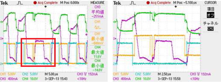
-----------------------------


-CH1:outC

-CH2:outD

-CH3:current flowing through the primary winding of power transformer

-CH4:pulse transformer(primary side)

-----------------------------

Is it probable function that outC/D lock up regardless of outA/B waveform is normal?

I think outC/D is associated with outA/B, and outC/D doesn’t lock up independently.

Could you advise me please?


I’m sorry that I can’t get schematic of the board(it is my customer’s matter).

The condition of DCDC converter board is Vin=270-280V, Vout=28V/50A.

Regards,

Yaita

  • Hi,

    Could you advise me about the matter?

    Please let me know if you need more information.

    Best Regards,

    Yaita

  • Hello team,
     
    I'm Ryuji Asaka, colleague with Yaita-san.
    Please kindly let me know the  below about UCC28950 issue.
    I got the customer's schematics, so if you need it, please contact to me directly.
    I can send the schematic by email
     
    (1)
    In the our customer, OUTA and OUTB are normal operation.
    But OUTC and OUTB are pulse skipped. (Please see the Yaita's first post as waveform)
     
    <Conditions>
    Vin=270-280V, (they tested Vin=260 to 400V, but pulse skip occur at 270 to 280V)
    Vout=28V 
    Iout=50A(1.5A/us , ΔI =49.5A) 
    RTmin=13k ohm ( same with minimum allowed restor on TMIN)
    OUTE, OUTF pins are open.  They don't use Synchronous Rectification.
    DCM pins connect to Vref.
     
    Are there any possibility of the OUTC, OUTD pulse skip at the above conditions ?
    If yes, please let me know the reason 
    Possibility is OK for us. 
     
    (2)
    If you have other case of pulse skips of OUT C and OUT D, could you please send the information?
     
    Best Regards,
    Ryuji Asaka
     
  • Hello,
     
    Sorry for bothering you.
    But could I have your coment please ?
    If you can't reply these information only, please let me know the necesarry information.
     
    Best Regards,
    Ryuji Asaka
  • When the duty cycle is less than the programmed on Rtmin the device goes into burst mode and gate driver pulses can be missed.  I believe this is what is happing.

    Regards,

    Mike

  • An example of burst mode is shown in figure 23 of the User's guide showing the missing pulse.  http://www.ti.com/litv/pdf/sluu421a

    Regards,

    Mike

  • Hello Mike san,

    Thank you for the reply. If this is occurred by less than rtmin , can we avoid this pales missing? 

    Since Rtmin is minimum value 13kohms now, they can not reduce rtmin value.

    best regards,

    ryuji asaka

  •  Unfortently you can't disable burst mode.  That has been a major complaint with this device.

    The UCC3895 does not have the burst mode feature if your customer desires to use FSFB controller without burst mode.

    Regards,

  • Hello Mike San,

    Thank you. I understood.
    Could you please kindly the burst mode mechanism at last?  
    (1)
    In customer, burst mode is occured about 280v. 
    Do not occur at the 270vin and 290vin moreover.
    Why burst mode is occurred at the 280v?
    (2)
    I understood that at the dynamic load changing , duty cycle will be decreased less than tmin.
    thus device operate burst mode.
    is my understanding correct?
    if yes please let me know this mechanism?
    Im sorry for the basic question...but please kindly let me know the information.
    best regards,
    ryuji asaka
  • What made believe this was burst mode is that test conditions were 500mA to 50A.  At light load the converter could be going into burst mode.  You just need to look at the duty cycle to see if this is the case. 

    Not sure why it is not occurring at 270 and 290, and only occurs at 280. 

    Regards,

  • Hello Mike san,
     
    At the customer, this occurs only about Vin-280V... (attached for your reference)
    This operation is not occured by 500mA.
    Occured by dynamic transient response and specific Vin.
     
    Our customer commented duty cycle may be 100%...
    Is burst mode caused of 100% duty cycle?
    If yes, we can avoid this operation by changing turns ratio of transformer ? 
     
    I will check the OUTA, B, C, D waveform to our customer for more information.
    But pleaase let me know.
      
    Best Regards,
    Ryuji Asaka
  •  Hello Ryuji,

    The map that you have attached shows that condition most of the behaivor happens at load steps of 0.5 to 50A.  At 0.5 the converter maybe calling for burst mode.  You could also be hitting peak current limit.

    Regards,

  • Hello Mike san,
     
    I think that OUTA , OUTB, OUTC, OUT D will be off under the burstmode.
    In the datasheet figure 2 , OUT A, B, C, D are off.
    But in customer operation , OUTC is High and OUTD is Low.
    I think that this is not burst mode.
     
    In the burst mode,  OUTC will be High and OUTD will be low ?
    If yes, I will inform this operation caused by Burst mode.
     
    If no, please let me know the assumed cause of this operation?
    If we can't identyfy by current information, please let me know should we check...
     
    Please see the attached file as waveform.
     
    Best Regards,
    Ryuji Asaka
  • There are only two functions that will cause abnormal gate drive.

    1. Burst mode, Duty Cycle is less than Rtmin

    2. Peak current limit

    If it is not either of these you might have layout issue. 

    Regards,


  • Hello Mike san,
     
    Thank you.
    I understood.
     
    Best Regards,
    Ryuji Asaka
  • Hello Mike san,
     
    This gate operation is not occured when our customer use low value Rcs.
    Please see the below picture as pulse skip wave form.
    This waveform is result of Cycle-by-Cycle Current Limit Current Protection and Hiccup Mode of the UCC28950.
    Thus, this behavior is along the datasheet.
    Is my understanding correct ?
     
     
    Best Regards,
    Ryuji Asaka
  • Hello Mike san,
     
    I got the new information for FET gate skipfrom our customer.
    Could you please let me know your answer?
     
    <Question>
    1: Are transformer saturation occured when Current limit and Duty limit occured same time?
    2: If yes are there any workaround?
     
    <Requirement Specification>
    Vin : 230V to 470V
    Vout : 28V
    Iout : 50A
    Fsw : 100kHz
    Rtmin=13kohms
     
    <Background>
    Our customer reviewed transromer saturation as following.
     
    They set the current limit as30A , Vin 230V and Vout 28V,
    They Increase the Output current from 0A to 50A
     
    Firstly ,Output voltage is decreased from 28V when Output current about 20A by duty limit.
    There is no transformer saturation in this point. 
    Secondly , ttranformer saturation was occured at the point of Iout 30A.
    In this point, Duty limit and Current limit were ooccured at same time( or within 30ns)
    Thrdly, transformer saturation is not occured at the Iout over 30A.
     
    They think that the transformer saturation is occured when current limit and Duty limit occured same time.
     
    Best Regards,
    Ryuji Asaka


  • It looks like the load step transient is causing the UCC28950 to misfire and cause the output C to turn on when it should be off. Please look at the drive outputs A,B,C,D. Check the layout of the gate drives and see that the ground to the UCC28950 is not directly connected to the power ground of the system.