This thread has been locked.

If you have a related question, please click the "Ask a related question" button in the top right corner. The newly created question will be automatically linked to this question.

LM25037 duty cycle

Other Parts Discussed in Thread: LM25037

Hi

I evaluate the LM25037 EVM which is modified to lower UVLO threshold  (R4 9.76kohm -> 15kohm) .

I obtained a strange behavior which is following duty cycle. 

There are large changes of the duty cycle for the variation of the input voltage(Vi=11V -> Vi=10.7V).

Why does this phenomenon(large changes of duty cycle) occur?

Regards,

Koji Hamamoto

  • Hello K,

    You need to check the uvlo leakage current, Iuvlo. The maximum value is listed on page 4 of  LM25037 data sheet. It says the leakage current out of this pin can get as high as 26 uA. The sink voltage is 0.6V, this means there is a maximum parasitic resistance of approximately 23 kohms in parallel with you 15 kohm. This drags down the value of the 15 Kohm voltage and causes your circuit to go into UVLO at a higher input voltage than you planned.

    If your chip has a worst case Iuvlo of 26uA and a Vsink of 0.6V, you have an effective leakage resistance of 23 Kohms in parallel with your 15 Kohm bottom resistor. This will cause you to go below the UVLO threshold of 1.23 V at an input voltage of 14.8 Vs.

    The 26 uA is a worst case maximum, so it appears you have only about 6 uA of leakage at that pin. So your UVLO trip point is around 10.7V. 

    With a minimum of 0.35 uA  Iuvlo leakage it's about 9.5 Vs. So 6 uA of leakage current raised the UVLO threshold 1.2 Vs.

    You need to account for this leakage current when you design you voltage divider. It may not be as high as the data sheet since this is a worst case maximum.

    Hope this helps

    Chuck

  • Hi Chuck-san

    Thank you for your support.

    I understand the the leakage resistance affect the uvlo threshold. I will try to measure the leakage current ,but it will be hard to measure.

    Also I have some question for your answer.

    Q1. How did you calculate input voltage(10.7V and 9.5 Vs) at the following cases?  

      [Your Comment] The 26 uA is a worst case maximum, so it appears you have only about 6 uA of leakage at that pin. So                                   your UVLO trip point is around 10.7V. 

                ( (6uA + (1.23V/15kohm))*100kohm  + 1.23V) = 10.03V?  Where the 6uA come from?

      [Your Comment] With a minimum of 0.35 uA  Iuvlo leakage it's about 9.5 Vs. So 6 uA of leakage current raised the                                       UVLO threshold 1.2 Vs.

                What is 0.35uA?

    Q2. As I asked at last post,why Duty has changed greatly at around UVLO threshold? What is the relationship between the deviation of the above threshold?


    Our customer will use LM25037 on their product. We need your support.

    Regards,

    Koji Hamamoto 

  • Dear Koji,

     [Your Comment] With a minimum of 0.35 uA  Iuvlo leakage it's about 9.5 Vs. So 6 uA of leakage current raised the                                       UVLO threshold 1.2 Vs.

                What is 0.35uA?

    I apologize for misreading the data sheet. I incorrectly read the 0.35 V Under-voltage Shutdown threshold 0.35 V as the minimum hysteresis current. So you are right the minimum current sink when the device is in shutdown is 17 uA. Of course you are not in shutdown so this current does not apply -my mistake. 

    Your question:

    "I understand the the leakage resistance affect the uvlo threshold. I will try to measure the leakage current ,but it will be hard to measure."

    I wouldn't bother to measure this current. Your voltage divider already is measuring it. The amount of leakage current into the UVLO pin will be proportional to the difference between the ideal voltage threshold,and the actual UVLO voltage threshold. What you need to do is check at what input voltage you are actually going into UVLO standby mode (less than 1.25 V +/- 0.05V. If your circuit is about to enter this shutdown mode, this could be what is causing the gate drive duty cycle to behave strangely. I would adjust the UVLO voltage divider until I had about 250 mV of margin between the UVLO voltage standby threshold and the minimum input voltage operation.

    I still suspect the UVLO threshold voltage is the source of the problem with your gate drive. Have you checked the gate drive pulses with the original voltage divider set for the original under voltage threshold?

    [Your Comment] The 26 uA is a worst case maximum, so it appears you have only about 6 uA of leakage at that pin. So                                   your UVLO trip point is around 10.7V. 

                ( (6uA + (1.23V/15kohm))*100kohm  + 1.23V) = 10.03V?  Where the 6uA come from?

    Please ignore the above calculation I made. It is in error due to my misreading of the data sheet. I assumed the 0.6V applied to standby mode UVLO condition. The voltage and leakage current of the UVLO pin are not listed when the device is in standby mode. However, there is always some leakage into an IC pin that must be accounted for, and this may cause the converter to go into the standby mode at a higher input voltage. When the device is in standby mode the IC's regulators remain active but the PWM output shuts down. What you are probably seeing is the beginning of the PWM output shutting down.

    Good luck,

    Chuck

  • Hi Chuck-san

    Thank you for your reply.

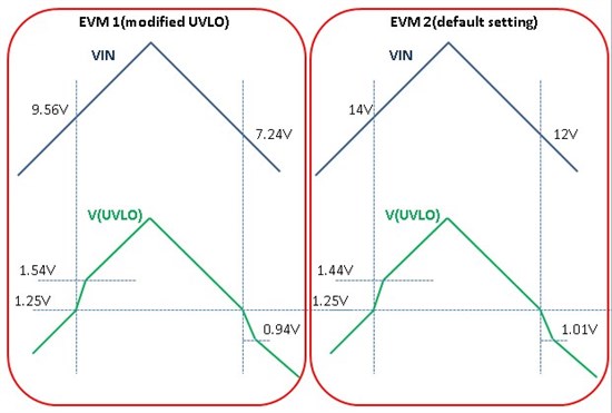
    I measured the voltage of UVLO pin and VIN pin when it is rising and falling.Please the following image.

    (I have two LM25037EVM. EVM 1 is modified UVLO threshold(R2=15k). and EVM 2 is default setting.(R2=9.76k) ) 


    By the way, I read the Application Note which is AN-1861. However there are some differences between typical application circuit and actual EVM board. (R2,R7,R8 and other components) Why does the value different?

    Regards,

    Koji Hamamoto

  • Koji,

    R2 controls the current used to charge up the Vcc pin cap. So maybe in the "typical" schematic they chose a better value for efficiency after some testing. R7 is the R part of the current sense RC filter so maybe they had to adjust it to keep it from shark toothing the input signal at very high load or not having enough noise rejection. And finally R8 is a part of the compensation network. It is used to form a pole with C11 and a zero with C8. So probably they had adjust these values to make the circuit stable.

    I also noticed that the specification on that apnote for the eval unit list the input voltage range for regulation from a minimum of 16 V to 32 V. And the same specification shows the UVLO trip voltage at 14 V, just like you have in your scope plots. So that means that from 14 V to 16 V, they do not guarantee regulation. I think that is your problem. Or actually you don't have a problem. You set your new UVLO trip point to 9.56 V. So you should leave 2 V margin for the minimum input of regulation. That means you now have an minimum input voltage of 11.56 V. So when you go below that voltage, your converter starts to go into standby mode. In other words, you need to set the UVLO trip point 2 Vs below the design minimum input voltage for regulation.

    I've used TI eval units before. We had to do a few modifications to make the design acceptable for medium volume production. They are only reference or "evaluation" designs. So you have to analyze them pretty hard before you finalize them as a production worthy unit.

    But it is a good start,

    Chuck

  • Chuck-san

    I appreciate your kind support.

    Please let me ask just three question.

    #1. Could you give us the value of  the components which is chaned from typical application circuit. (especialy capacitance.) The customer would like to set the same value on thire board.

         R2,R7,R8 and C???

    #2.As you mentioned, 'In other words, you need to set the UVLO trip point 2 Vs below the design minimum input voltage for regulation.' I do not understand what does it happen if the VIN fall below the margin of the 2V. At the EVM-2 the abnormal duty cycle which is occured at the EVM-1 is NOT occured.

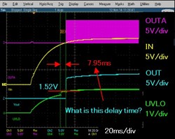
    #3. I have found some deley time when it is startup. Please see the following image.


    Regards,

    Koji Hamamoto.

  • Koji,

    Your questions below:

    #2.As you mentioned, 'In other words, you need to set the UVLO trip point 2 Vs below the design minimum input voltage for regulation.' I do not understand what does it happen if the VIN fall below the margin of the 2V. At the EVM-2 the abnormal duty cycle which is occured at the EVM-1 is NOT occured.


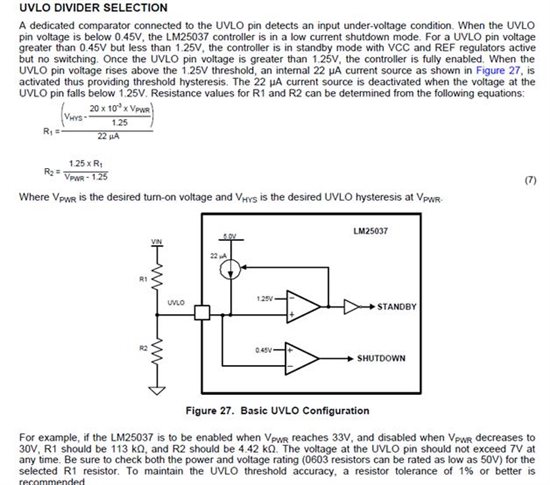
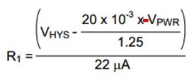
    If you look at the UVLO divider selection shown above, you will see how the voltage divider components are selected. There is a current source that influences the UVLO trip point so that it trips "on" at on one voltage and "off" at a lower voltage. So in the case of the original design, the converter turns "on" at 16 Vs, but trips "off" at 14 Vs. So they have designed the UVLO to have 2 Vs of "hysteresis". You need to use these equations to select your divider components. 

    As far as the abnormal duty cycle phenomena, I have no idea why that is happening. Probably the only one who knows that is the IC designer. It could be that the 22uA current source is turning on too quickly or overshooting and modifying the duty cycle. It could be that the IC's gate driver section has a problem. The only way to know is to change out the PWMIC and test. But if the duty cycle problem is occurring at a voltage below the minimum operation voltage, does it matter?

    By the way, I read the Application Note which is AN-1861. However there are some differences between typical application circuit and actual EVM board.

    #1. Could you give us the value of  the components which is chaned from typical application circuit. (especialy capacitance.) The customer would like to set the same value on thire board.


    What I was trying to say was that the components on the EVM board may be different from the typical application circuit because TI had to make some minor changes from the initial design-the typical application circuit. These changes could be due to testing that showed there were problems like the ones that I mention in the last message. So the component values on the evaluation board are the correct ones and I wouldn't change them. 

    The above is only true if they are different because of some tuning required after building the prototype. Your customer needs to test the design and make sure it is working properly in the areas where the component values are changed. I don't know what the component values are in the actual evaluation board. 

    It is possible that TI simply put the wrong parts on the board. If that is the case you need to contact them. Or you can test. 

    #3. I have found some deley time when it is startup. Please see the following image.


    Start up delays are normal in my experience. The output filter inductor and capacitor has to charge up. 7 ms sounds normal to me.  It also takes some time for the PWMIC to reach it normal operating voltage.

    Hope this helps,

    Chuck

  • Hi Chuck-san

    I appreciate your kin support. These were very helpful for me.

    If you look at the UVLO divider selection shown above, you will see how the voltage divider components are selected. There is a current source that influences the UVLO trip point so that it trips "on" at on one voltage and "off" at a lower voltage. So in the case of the original design, the converter turns "on" at 16 Vs, but trips "off" at 14 Vs. So they have designed the UVLO to have 2 Vs of "hysteresis". You need to use these equations to select your divider components.

     Thank you for your explaination. Only the modified R2 is caused this problem.

    Start up delays are normal in my experience. The output filter inductor and capacitor has to charge up. 7 ms sounds normal to me.  It also takes some time for the PWMIC to reach it normal operating voltage.

    OK. Can you give us how much does the delay have a variation?


    Reagards,

    Koji Hamamoto


  • Hi

    I am sorry for many question.

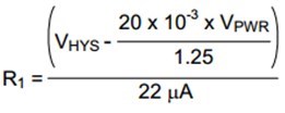
    I checked UCLO trip point by equation below.

    I think the equation must be below,

    *: It should be (-VPWR) since on the evaluation R1 is 100kohm and VPWR is 14V, VHYS is 2V.


    What do you think?

    Regards,

    Koji Hamamoto

  • Hi Chuck

    I explained to the customer about this issue. They understood.

    Please let me close this issue.

    Thanks

    Regards,

    Koji Hamamoto