This thread has been locked.

If you have a related question, please click the "Ask a related question" button in the top right corner. The newly created question will be automatically linked to this question.

LM25037 delay time and soft start

Other Parts Discussed in Thread: LM25037

Hi

I have two question for this device.

Our customer will use this device without feedback loop at isolated push pull controller application.

1. Dose this device have implemented soft start time when the FB pin is connected to GND?

     I though this soft start operation does not work when FB pin is connected to GND. However it looks soft start operation is working during it is starting up. (It is not max duty cycle.It is narrow duty cycle such as 740ns on time.)

2. This device has delay time to start the switching operation. What time is the typical and maximum value of the delay time?

Regards,

Koji Hamamoto

  • Hi

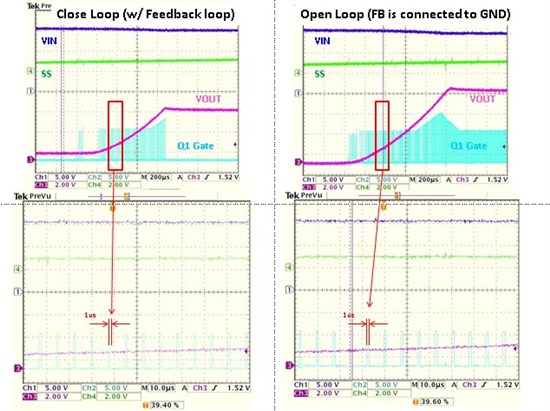
    I evaluated the two EVM to compare with no-feedback loop version and normal(= with feedback loop) version.

    EVM-1. Close loop : It is default setting such as TI-EVM.

    EVM-2. Open Loop : It is modified only the feedback loop. It is without loop compensation and FB is connected to GND.

    There are same soft start operation.

    Why does EVM-2 operate with soft start? Does the EVM-2 operate with soft start even if the FB is connected to GND(soft start disables)  

    Could you provide your answer about the soft start and the delay time (my previous question)? 

    Regards,

    Koji Hamamoto

  •  

    If you look at the IC block diagram on page 8 of the LM25037 datasheet, you can see that there is no dependency between the FB pin and the SS pin.

    If the FB pin is connected to GND, this will force the error output (at the COMP pin) to go high, through the 5 k internal pull-up to the internal 5 V rail, as shown.

    The SS pin is internally shorted to GND by the "Shutdown" internal signal until all internal IC power good conditions are ok (VCC ok, VREF ok, etc). The SS pin voltage is connected to the "SS Buffer", shown below the COMP pin. This buffer will independently pull down the COMP pin to force the COMP pin to track the SS pin, until the SS pin increases above the COMP level, then the COMP level is controller only by the error amp. This is because the SS Buffer open-drain output can only pull-down the COMP, it can cannot pull it up.

    So after the "Shutdown" signal goes low (when all internal rails are good), the SS pin external cap is charged through 100 uA current source. The dv/dt on the SS is matched at the COMP pin by the "SS Buffer" circuit. When COMP level exceeds the 1 V offset, then the PWM starts, with narrow pulse width, and the pulse width increases as COMP & SS rise together.

    Since the COMP & SS pins have to charge from zero to the ~1 V internal offset before the PWM starts, this causes a delay. This delay will depend on the value of the SS cap, and can be calculated from the cap value, and the value of the internal 100 uA charging current source. Nominal delay is 10 us for every 1 nF of capacitance on the SS pin.

  • Hi Bernard

    Thank you for your reply.

    That was very useful! I talked customer about the your comment. They understood.

    Thanks again.