This thread has been locked.

If you have a related question, please click the "Ask a related question" button in the top right corner. The newly created question will be automatically linked to this question.

UCC27524A Data sheet is unclear about the functionality of the Enable pin

Other Parts Discussed in Thread: UCC27524A, UCC27511

Reviewing the UCC27524A data sheet, I am confused as to the functionality of the ENable pin.

The drawing on page 1 shows the buffer as I would expect a Tri-State buffer to be drawn

BUT

The functional block diagram section 8.2 indicates that it is AND'd with the Input signal.

Section 8.3.3 says "Thus when ENx pins are driven high the drivers are enabled and when ENx pins are driven low the drivers are disabled."

BUT

Section 8.4 shows that when ENable is low the Output is low

  What is the actual functionality of the Enable input?  Does it cause the output to go into high impedance condition or is the output driven LOW?

-Phil-

  • Hi Phil,

    The table in Section 8.4 is the clearest clarification.

    In section 8.3.3 "Thus when ENx pins are driven high the drivers are enabled and when ENx pins are driven low the drivers are disabled." it means that when ENx ARE low then the output of driver are driven to low despite the level on INx. When ENx are driven high, then the status of OUTPUT of driver are decided by the INx.

    br

    Kening

  • So the functionality is that of an AND function. If either input is LOW then the output is LOW. If BOTH inputs are high then the output is HIGH. The ENx input is not an ENABLE it is simply the second input to the AND.

    Can you recomend a device that offers a similar driving capability and has a true ENABLE (causing the output to high impedance) functionality?
  • Hi Phil,
    So your need is: when ENABLE is low, then the output is high impedane despite of the Input?
    Why you need such a function?
    Usually customer like a certain output status(high or low). Because if the output is high impedance when it is driving MOSFET, the gate is easily be affected by noise to go to high or some unexpected floating level.
  • The implementation is not standard and is for a test system. What I need is a device that is able to provide EITHER an OPEN-DRAIN or OPEN-SOURCE buffer/driver. Low speed (<5KHz) with > 500mA of drive and tolerate 5<>18v. I was intending to use the INPUT to define the OPEN-DRAIN or OPEN-SOURCE and then control the ENABLE to cause the output to be driven of floating. Thus for an OPEN_DRAIN I would have the input LOW (assuming a non-inverting buffer) and connect the ENABLE signal to the controlling source. Enable active >> Output driven LOW. Enable inactive >> Output OFF.

    My confusion was with the use of the term enable or disabled. I was expecting a disabled output to NOT be driven but to be in a high impedance state (3-State).
  • Hi Phil,

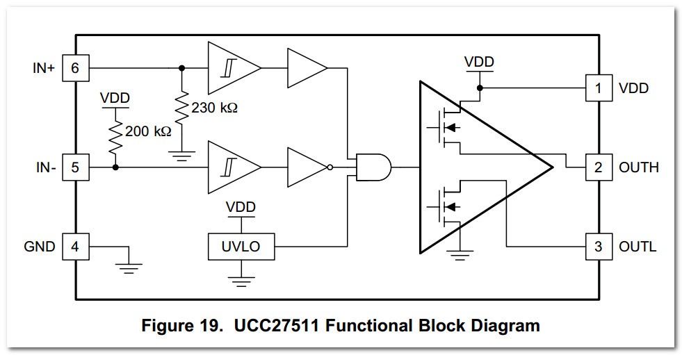
    May you look at UCC27511.

    I cannot find oter parts except this one.

  • That looks it will fill my needs nicely. I appreciate the suggestion.
    -Phil-