This thread has been locked.

If you have a related question, please click the "Ask a related question" button in the top right corner. The newly created question will be automatically linked to this question.

Bootstrap capacitor voltage drop LM5106

Other Parts Discussed in Thread: LM5106, LM5109B-Q1, LM5105

Hi all,

Just a question on the bootstrap capacitor voltage drop as I am using the LM5106 datasheet, but something seems not clear.

On the value for the boot capacitor for my application, I can calculate it like: Cboot=Qgtotal/VHB, being

Qgtotal = 93nC (maximum value), the total gate charge for my IPP075N15N3G MOSFET

VHB = 12V (driver dc supply) - 1V (boot diode voltage drop) - X? (X is this the mosfet Vgsmin? or what else?)

The formula in the LM5106 datasheet says that where I put X above I should use the MOSFET Vgs,min which for my switch is 4V.

However, another TI document for LM5109B-Q1, says that where I put X in the formula above I should use VHBL = VHBRmax – VHBH which are values related to the undervoltage protection.

The question is, what should I use for X in the VHB formula, and why? I am using LM5105 as gate driver.

Thanks a lot,

Leo

  • Leo,
    Thanks for you interest in TI here. Ive contacted the product group. Look for an answer from them soon.
    Regards
    John
  • Hello Leo

    I tend to agree with you - the Datasheet isn't clear. However there are only a few rules to follow here -
    1/ The voltage on the bootstrap capacitor must remain above the UVLO threshold of the driver after the MOSFET gate has been charged.
    2/ In practice this means a charge on the bootstrap capacitor which is at least 10 times greater than the charge needed to turn the MOSFET on - in your case, 93nC x 10 = 930nC at 11V = 84nF. I would suggest a 100nF part here. The bootstrap cap will lose about 10% of its initial voltage as it charges the MOSFET gate.
    3/ The local bypass capacitor, from VDD to Ground should be at least 10 times the value of the bootstrap capacitor - in your case I would suggest a 1uF part.
    4/ You may need to add a current limiting resistor in series with the bootstrap DIODE so that the charging currents supplied from the bypass capacitor to the bootstrap capacitor remain within the bootstrap diode peak current ratings. Try to use a resistor around 2 Ohms here. If the resistor is too large, then the bootstrap capacitor initial charge will take too long (you should be charging the bootstrap capacitor from 0V to >UVLO in less than one switching period). BTW, the resistor will have to carry high pulse currents - make sure it is rated for these (or as a rule of thumb use 1206 size parts.)
    5/ The single most important thing is the PCB layout around the driver. The suggested component layout in Figure 21 is a very good starting point. The bypass capacitor, CVDD should be placed as close to the VDD and GND pins as possible. The bootstrap capacitor should be placed as close as possible to the HB and HS pins. The charging path through the diode and resistor from VDD to HB should be low impedance (short).
    6/ Use good quality (X7R) capacitors for Cbootstrap and Cbypass and check that the parts you are using have a low voltage co-efficient of capacitance. (50V parts are usually ok)

    These guidelines will get you a working system - it is not usually worthwhile trying to put in smaller capacitors - there is no cost saving to be had and performance may be degraded.

    Again - on PCB layout
    Keep the path from HS through to the source of the high side MOSFET as direct as possible.
    Keep the path from HS through the drain and source of the Low side MOSFET and back to VSS as direct as possible to minimise negative going transients on HS

    Regards
    Colin
  • thanks Colin, your answer is very useful.

    The only doubt I still have is on point 4. As my gate driver is fed by a current limited +12V supply (a TRACO TEN 30-2431). The current of this supply seems to be limited to 150%*0.42A, after that the power supply protection will kick-in. I was considering using perhaps a NTC resistor, in order to decrease the boot diode/capacitor circuit inrush current at the startup, so once the resistor gets hot, its resistance goes down, and the boot diode/capacitor circuit keeps absorbing a current which is below the limit of my +12V supply. Do you think this would work?  Or do you have any suggestion for the NTC resistor I can use?

    Thanks again indeed,

    Leo

  • Hello Leo

    The average current from the Bias rail is going to be small (10mA to 20mA perhaps) - and well below the 460mA that the TRACO device is capable of supplying so I don't think you need to worry about inrush current limiting at all. Also, all supplies have to be able to startup into a capacitive load which may cause them to run into current limit in the normal course of operation.

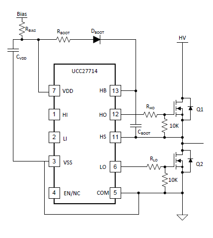
    The resistor Rbias (below) is not for inrush current limiting at all, its function is to provide a RC filter network so that variations in VDD due to MOSFET switching action do not get passed onto the Bias rail. Typically a 10 Ohm resistor is used here but you could go higher (20 or 30 Ohms) if you needed to limit the current from the TRACO source. An average driver current of 20mA would drop 200mV in a 10 ohm Rbias resistor

  • Thanks Colin, actually I have checked the Traco datasheet but it does not mention about startup on capacitive loads. I am afraid that the inrush current to charge Cboot may be an issue, as it will trigger the traco converter protection. I have been suggested to use an NTC resistor or perhaps a ferrite bead(?) to limit such inrush current, but I am not sure on how to choose these components. My Cboot capacitance is 270nF charged by the +12V  of the traco. Not sure if it is a useful info, however the mosfet I am switching using the TI driver LM5106 has a gate charge Qg of 93nC.  If you have any suggestion for selecting a NTC or a ferrite bead to connect in series with the boot diode and thus limit the inrush current it would be great. Thanks again,

    Leo

  • Hi Leo

    In the small print at the end of the Traco DS there is a section called 'Capacitive load output models' and it gives a 220uF max cap load on the auxiliary outputs so this is the limit I would obey. the DC/DC converter should happily start up into this size of capacitor.
    The 270nF bootstrap capacitor is charged from the stored charge in the capacitor at the VDD pins (Cvdd should be REALLY close - eg AT - the VDD and GND pins of the driver). In any case, this capacitor is not normally charged until the first LO pulse comes along and pulls the HS pin to ground. The Traco PSU won't supply the high frequency charging pulses needed by the bootstrap capacitor for a couple of reasons - 1/ Any DC/DC converter will be much too slow to supply these HF pulses and 2/ It will be much too far away.
    Basically, you don't need to worry about inrush currents from the Traco.
    In any case an NTC won't work because in normal operation there is insufficient current to keep it hot.
    The only thing you may need is a resistor in series with the boot diode to limit peak currents in the boot diode itself - typically a part somewhere between 1 and 2 Ohms would be fine (use a 1206 size part)

    Regards
    Colin
  • Hi Colin, thank you very much indeed.

    I did not know the meaning of the TRACO datasheet section 'Capacitive load output models', that is true for the auxiliary output (i.e. +/-12V) it gives that 8000 +/-220uF, I did not know how to interpret that part of the datasheet.

    I will take that as the maximum capacitive load the DC-DC can start-up with I suppose.

    Probably then all I will do is add a 2 ohm resistor in series with the boot diode.

    Best regards,

    Leo
  • Hello Leo

    Yes, that's the way I would interpret the Data Sheet. 2 Ohms in series with the bootstrap diode is a good value to start with.

    Regards
    Colin

  • Thanks Colin, it is very great advice what you gave me.

    Best regards

    Leo

  • Hi Colin,

    Thanks again for your valuable answers.

    I am still designing this circuit and I was wondering, on your suggestion of using an Rbias as per the above picture. Does it perform a sort of RC filtering with CVDD, in order to get rid of switching noise from entering the VDD terminal?

    Also, is Rbias slowing down the charge of Cboot (when Q2 is turned on) and therefore influencing the minimum time I have to hold Q2 in the ON state to fully recharge Cboot?

    Just out of curiosity, is it the same thing if rather than using Rbias I use a ferrite bead (connected between the same terminal?)? let's say Fair Rite PN 2773021447 (EMI Filter Beads, Chips & Arrays 73 SM BEAD Z=78 OHM @25MHz).

    My power stage switching frequency is 200kHz...

    Thank you very much again.

    Leo
  • Hi Leonardo

    Rbias won’t affect the charging rate or time of Cboot. Cboot is charged from CVDD (which is why CVDD is at least 10 times larger than Cboot). You can certainly use a ferrite bead, the one you mention has 25 Ohms impedance at 25MHz and a DC current rating of 5A which is more than adequate. The bead will be more expensive than the resistor and you will have to decide if the slightly better performance is worth the cost.

    Rbias does form a RC filter with CVDD to filter noise on the bias rail.

    The charge needed to turn Q1 on (total gate charge) has to be delivered into Cboot during the minimum Q2 on time. So: You need to look at the minimum Ton time of Q2 and whether Cboot can be re-charged during this time. The following factors affect this:

    The speed of the boot diode, forward recovery time especially:

    The value of the current limiting resistor, Rboot:

    The impedance of the current loop from CVDD to Cboot and back (PCB layout).


    Regards

    Colin

  • Hi Colin,

    Thanks again for your answer, it really really helps.

    I think I will choose the Rbias=10Ohm over the ferrite bead, as I am not sure about the frequencies I need to suppress, and a Rbias of 10Ohm (combined with CVDD=3.3uF) will filter all frequencies above

    which makes me think that switching ripple at 200kHz (my switching frequency) will surely be filtered. With the ferrite beads,, while their impedance is spec'd for the MHz range,  I am not sure of their filtering behavior for frequency close to 200kHz.

    In regards to the minim on-time for the low side switch, I still have some doubts, as the information I found on line is not always simple to apply. Hopefully you or someone in this forum can help...

    1) From my understanding, here is how I choose the boot capacitance value for LM5106, driving an half bridge using IPP075N15N3G MOSFETs (having Qg=93nC, let's say 100nC to round up):

    Where 1V is the drop on the boot diode, 12V is the VDD supply to the driver and 6.9V is the UVLO threshold (in the above I have disregarded any voltage drop on eventual boot resistor). Cboot ~ 24.4nF, say I choose Cboot = 330nF, and consequently CVDD = 10xCboot = 3.3uF.

    With these values (Cboot=0.33uF, CVDD=3.3uF, VDD=12V), let's say I put a Rboot = 2ohm, I still don't understand how to calculate the minimum on time of the low side switch needed to replenish the charge in the boot capacitor.

    If I don't consider Rboot for simplicity, and the voltage drop on the boot capacitor is:

    Now, the minimum charging time to replenish this voltage drop is (minimum on time for the low side switch):

    so the minimum duty ratio is, the Dt calculated above divided by the switching period (5us), but  I am not sure of what to use as I_Cboot here, is this current coming from the CVDD capacitor? 

    2) Furthermore, if I now consider a Rboot =2 ohms in series with Cboot, I am not sure how this influences the minimum on-time I must have for the low side switch (in order to recharge the bootstrap capacitor). Some literature, says that the minimum (on-time) duty ratio needed for the low side switch must be:


     which unfortunately does not make a lot of sense to me, as it sounds too large...

    In summary, I am looking for how to roughly estimate the minimum on-time constraint (re: replenishing boot capacitor charge) for the lower switch, having a Cboot=0.33uF, CVDD=3.3uF, VDD=12V, Rboot=2 ohm (0.5W), and as a Dboot I was planning to use a schottky diode (ON SEMICONDUCTOR MBR2H200SFT1G) and using IPP075N15N3 G MOSFETs, with the Texas Instruments gate driver LM5106. 

    Thank you very much again,

    Leo

  • Hi Leo

    The noise at the CVDD is caused by the pulse of current fed into Cboot each time the Bottom MOSFET (I’m going to call this part Qbot) is on. There will be some additional noise due to capacitive coupling from the switched node (Qbot Drain) onto CVDD but careful layout will minimise this and in any case it won’t be the main noise source. What this means is that the waveform you are trying to filter is a series of short duration, high speed impulses with a 400kHz repetition rate. Most of the energy will be at high frequency harmonics of this repetition rate rather than the fundamental so the RC network (Rbias and CVDD) has to filter high frequency impulse noise rather than a waveform at 400kHz. This is the reason the ferrite beads would be effective. Don’t forget that the PCB layout can introduce parasitics (R in series with CVDD, and C in parallel with Rbias) that can completely alter the transfer function of the simple RC filter and reduce its high frequency attenuation significantly. PCB layout is key here.

    Your MOSFET, IPP075N15N3, has a total gate charge of 93nC so this charge has to be supplied from Cboot each time the MOSFET is turned on. In the steady state this is also the charge that has to be put back into Cboot during the minimum Ton of the Qbot. You should charge the MOSFET gate to at least 10V, so let’s assume that this is the voltage on Cboot when Qbot is turned on. The voltage change on Cboot is Cboot/Qg or about 0.93V if Cboot is 100nF – so we need to charge Cboot to 10.93V. If Cboot is 330nF the voltage change is only 282mV and we need to charge Cboot to 10.28V. The point here is that you have about 1V available across Rboot to charge the 100nF cap but 1.72V available to recharge the 330nF capacitor, assuming 1V lost across Rboot. I ran some calculations and you can see that you need 250ns to recharge the 100nF capacitor but only 105ns to recharge the 330nF capacitor – it’s a little bit counterintuitive but the key is that the FINAL voltage on Cboot is the same.

    This charge/discharge is a high frequency process and your layout needs to minimise parasitic inductance in the out and return paths from CVDD to Cboot.


    The equation you have for Dmin is too conservative, use the equations above for Ic(x) for more realistic results.

    Don’t let the Cboot voltage drop to 6.9V because you will probably hit UVLO on the driver and you won’t fully enhance the MOSFET).

    Icboot does come from the CVDD capacitor.

    You can use the equation for Ic(x) above to recalculate for different values of Rb (Rboot) and Cb (Cboot).

    CVDD should be large enough that the charging of Cboot doesn’t affect its voltage – the 10:1 ratio between CVDD and Cboot is conservative. A larger Cboot will require longer for it’s initial charge at startup and Dboot will have to be rated for the peak current (12V in 1 Ohm in this case) but this is a peak value not a steady state value.


    The main thing you will need to think about is what duty cycle does the power stage need in order to provide the input / output conversion ratio you want. This calculation is the one that will set Dmin for you and you will then have to make sure that Cboot can be replenished in the available time.

    Do let me know if the image (equations) above don't display correctly -

    Regards

    Colin

  • OOPS - I just spotted a typo - I should have said Dboot - corrected below

    The point here is that you have about 1V available across Rboot to charge the 100nF cap but 1.72V available to recharge the 330nF capacitor, assuming 1V lost across Dboot.

    Colin