This thread has been locked.

If you have a related question, please click the "Ask a related question" button in the top right corner. The newly created question will be automatically linked to this question.

How to reduce the deadtime of TL594?

Other Parts Discussed in Thread: TL594

Dear TI Engineer,

I want to konw how to reduce the deadtime of TL594, according the datasheeet, if add the deadtime can through increase 4 pin voltage, so I need to reduce the deadtime whether may reduce the 4pin voltage to realize. Now, I have encounter two problem need the answers.

1)How to decrease the voltage of Pin 4? Because the inner have a 0.12V voltage source.

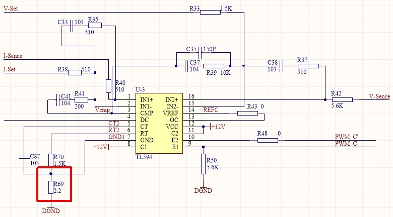
2)Whether can be add the 5Pin voltage to realized?  The SCH as below. I had test the PWM by oscilloscope, the deadtime actually decrease. Sometimes the chip will stop work, If reduce the R69 resistance to 1Ohm, the chip will work normally. I want to konw what causes the chip failure.

Waiting for your reply, many thanks!

  • Jacking Jin,
    Thanks for your interest in TI. I've contacted the appropriate product group that supports this device. You should hear from them soon.
    Regards,
    John
  • Hello,

    Could you please try to reattach the schematic? It did not seem to come through.

    In order to control the dead time, you can apply any voltage between 0 and 3.3V to set the dead time anywhere from 3% to 100%.
    Please refer to section 3.3.1 in the following application note: www.ti.com/.../slva001e.pdf
    The minimum deadtime for this device is 3%.
    Are you trying to reduce the deadtime further by increasing the baseline CT voltage?

    As for your second question, when you attach the schematic, I would be happy to look into this further for you
    Where are you putting the resistor?

    Best,
    Michael
  • Dear Michael,
    Thanks for your quickly reply.
    As you said, we can control the voltage to set the deadtime, but the chip set the minimum deadtime is 3%, whether can we change the deadtime to 1% or 2%?
    I had uploading the SCH in the body, but it's not display, I'm so sorry I don't konw how to process it.
    According the datasheet Figure 1, there have a deadtime control comparator, we're diffcultly to change the non-invert voltage, so we want to change the invert voltage to control the deadtime, that is by increasing the baseline CT voltage(the chip GND is floating relative the system ground). I don't konw the method is right or wrong.
    In the fact, through increasing the CT voltage, the deadtime is really decrease. but some time the chip may stop work, and you need power off and power on again.

    Waiting for your reply, many thanks!
  • Hello,

    When you are creating a new post, please select the "Use Rich Formatting" Button at the bottom right of where you are making the post. Once you select this it will bring you to a page where you can click the paperclip icon to 'Insert File'. If you try this, then maybe I will be able to see the schematic.

    Yes, based on the internal diagram, although I haven't seen it done before, it makes sense that you could offset the RT/CT pin voltage to decrease dead time.

    If you are using a resistor between the RT/CT and a ground, you should make sure that only the RT/CT is connected to the slightly elevated voltage. You should still connect the GND pin to the actual ground. If the GND pin is at the slightly elevated voltage as well then other pins that are connected to ground will be at a negative potential which could potentially cause issues.

    Does this make sense?

    Best,
    Michael

  • Dear Michael,

    Thanks! The SCH as below.

    The R69 use 2.2Ohm will be about 20% chance of failure, If change the R69 to 1Ohm, the system is still work, but the deadtime are not satisfy product design.

    In addition, Could you help me recommend a new chip of PWM controller for the design, because the TL594 max duty is only 45%, I have design a BUCK topological structure, the input voltage range is wide and hope the max duty can reach to above 70%.

    Thanks!

  • Hello,

    Yes, in this scenario you should try connecting the GND pin (pin 7) to the DGND voltage connected to the other side of the resistor. This way the device will be connected to the true ground, while the CT2 and RT2 pins will be connected to the slightly elevated voltage due to the drop across the 2Ohm resistor.

    As for the duty cycle you need, this device can actually due the maximum duty cycle if you operate it in parallel mode. If you connect pin 13 (OC) to ground instead of the VREF, then the outputs will be switching at the same time and they can actually switch up to 97% duty cycle (and potentially up to 100% with the offset voltage on the CT2/RT2 pins.

    For your buck converter, do you only need a single switch or do you require two switches?

    Best,
    Michael
  • Dear Michael,
    So I want to konw what cause use 2.2Ohm will stop work and use 1Ohm normally work. If we use the method to decrease the deadtime that is reliable?
    My buck converter is synchronous rectification, need drive two switches.

    Thanks!
    Jacking
  • Hello,

    The 2.2Ohm may cause enough offset that the negative voltage (relative to what GND is connected to) on other pins may cause the device to not function properly.

    The maximum duty cycle you can get out of each of these switches in push-pull mode of operation is about 47%, so if you need the duty cycle on the two switches to be able to go past that, then we need to find a new part.

    What are your input and output voltage requirements?
    What is the output loading?

    Best,
    Michael
  • Dear Michael,
    OK, I see. Thanks for your help!
    The converter voltage requirement, Input voltage: 7V~13V Output :5V/20A
    The PWM controller is not need integrated MOSFET. Thanks!
  • Hello,

    Have you tried our WEBENCH design tool before?

    webench.ti.com

    You can input your input and output voltage and current requirements and it will provide a suggestion for the best solution.

    Here is a link to some prefiltered results based on the conditions you provided:

    https://webench.ti.com/webench5/power/webench5.cgi?origin=ti_panel&lang_chosen=en_US&VinMin=7&VinMax=13&O1V=5&O1I=20&op_TA=30

    Best,
    Michael

  • Dear Michael,

    Recently, I have an idea that  I want design  volage follower as a voltage source to add the RT/CT, Do you think the method is feasible?

    Another,  Did the deadtime change is related with R&C value of the RT/CT pin?

    Many thanks!

  • Dear Michael,
    Recently, I have an idea that I want to design a voltage follower as a voltage source add to RT/CT. Do you think the method is feasible?
    Another question, Is it effection the deadtime change that the diffent R&C vaule of RT/CT Pin?
    Many thanks!
  • Hello,

    Were you able to try the method with the resistor to see if the deadtime was reduced? 

    In theory, if you increase the voltage at the RT/CT connection point, then it should reduce the deadtime. If the voltage follower fixes this voltage at a slightly higher voltage, then I expect the deadtime to decrease. If the offset is larger than the internal 0.1V, then the deadtime would be 0% of the duty cycle.

    Best,
    Michael