This thread has been locked.

If you have a related question, please click the "Ask a related question" button in the top right corner. The newly created question will be automatically linked to this question.

UCC27424 Output Impedance

Other Parts Discussed in Thread: UCC27424

Background:

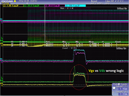
UCC27424 is presently driving SRs in a center tapped secondary application. During startup (1st 500uS), we noticed the VCC of UCC27424 was still zero volts, but the output pins were going to 2.1~2.4V. This might be  due to miller effect of the switching drain of the SRs.

Ch1: SR Vgs

Ch2: SR Vds

Ch3: Secondary Winding

Ch4: Primary Winding


Questions:

1.      When Vcc is 0V, what is impedance between UCC27424 output pins (OUTA/OUTB) and Ground?

2.      Will there be reliability concern on the UCC27424 if 2.1 volts difference between output pin and Vcc.


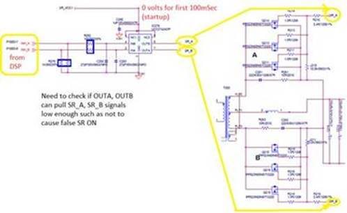
Reference data: Application circuit

  • Hi Andrew,

    Thanks for posting your question. I have contacted the HPDS drivers team and one of their engineers should respond today.

    Regards

    Peter
  • Hello Andrew,

    The rise in gate voltage as you mention is due to the miller charge coupling during the MOSFET VDS rising edge. The impedance of the UCC27424 to ground will be dominated by the high side (sourcing) MOSFET body diode which will clamp to VDD. As you mention the VDD is zero and has bypass capacitance, so the body diode of the internal driver MOSFET will clamp to VDD which is at 0 V.

    To comment on any reliability concern, can you provide the value of resistance in series with the gate of the MOSFET? I could not read the attached drawing value details.

  • There is 2.5ohms in series with the Gate.

    Based on below, it is possible to charge Vdd Bypass Cap thru this high side mosfet body diode. Therefore, Vdd shouldn’t just stay 0V. I think this will suffice for now. This should be problem with the application circuit that needs fix.
  • Update from customer:


    We eventually still need the OUT A/B impedance when Vdd level is not enough to turn ON UCC27424. By the way, I cannot see in the spec the UVLO or voltage when UCC27424 will turn ON. Does this part have this data OR just guarantee operation @ 4~15Volts? I’m thinking is it possible that I’m also charging the Vdd Cap through the body diode?


    For Mosfet, we have ~3ohms in series with Mosfet Gate.

  • I am confirming the output clamp circuit for the gate driver with low VDD voltage with IC design. For the questions about the UVLO, the typical performance is indicated in the Typical Characteristics curves Figures 21 thru 24. Fig 23 indicates the output starts switching at a VDD rising edge of 2V which is very low for a driver UVLO. Fig 24 indicates approx. 1.5V falling edge UVLO. The low UVLO operation should help mitigate the concern of the customer on dV/dt induced Vgs on the MOSFET.

  • Hello Andrew,

    After confirming the output clamp method is as used in most drivers, it is best to demonstrate the VOUT clamping voltage with a current source pullup on VOUT, and sweep VDD voltage from 0.

    The attached plot shows VOUT VS VDD with 3 different VOUT pullup currents of 1mA, 10mA and 25mA. You can see there is an internal clamping circuit that starts pulling down the driver with VDD from ~1V to 1.3V. VOUT is limited by the driver body diode to VDD until the clamping circuit is active.

    The setup is INA pulled to ground, adjustable current source on OUTA, VDD connected to variable supply with pulldown resistance in parallel.

  • Hello Andrew,

    Re post, graph did not insert on previous post.

    After confirming the output clamp method is as used in most drivers, it is best to demonstrate the VOUT clamping voltage with a current source pullup on VOUT, and sweep VDD voltage from 0.

    The attached plot shows VOUT VS VDD with 3 different VOUT pullup currents of 1mA, 10mA and 25mA. You can see there is an internal clamping circuit that starts pulling down the driver with VDD from ~1V to 1.3V. VOUT is limited by the driver body diode to VDD until the clamping circuit is active.

    The setup is INA pulled to ground, adjustable current source on OUTA, VDD connected to variable supply with pulldown resistance in parallel.

  • Follow ups from the customer:


    1.      Does this level increase as the pull-up current increases? Suppose the pullup current is not DC current but Spike current, what max Vout can we see?

    2.      What is the effective impedance in this section?

    3.      When Vdd is between 1.3V and 2.2V, the Clamp circuit drives Vout = 0 Volts (based on graph)?

    4.      What pull down resistance did you place between VDD and Ground? Please share the test circuit details other than description, thanks

  • Andrew,

    I will answer the questions as listed in the post.

    1) The voltage level will increase as the pull up current increases. The level of a peak current, Vs DC will be equivalent to the same DC level, but a short spike current should not charge the VDD cap significantly. The max Vout will depend on the current level.

    2) The effective impedance of the clamping at low VDD; below the 1 to 1.2V VDD where the VOUT is actively pulled to ground. Is the body diode comprising of a 0.5V VF and a 5.8 Ohm resistance clamping to VDD. This is based on total Vf measured from 1mA up to 50mA.

    3) That is correct, at VDD from 1V to ~1.3V the OUT pin is actively driven to ground.

    4) For the test, I placed a 5 ohm resistance from VDD to ground to achieve close to 0V VDD with the current source connected to OUTA pin.

    I am attaching the file of the test circuit, and an illustration of the effective body diode Vf and series resistance.UCC27424 OUT Clamp Test.pdf