This thread has been locked.

If you have a related question, please click the "Ask a related question" button in the top right corner. The newly created question will be automatically linked to this question.

LM25037 - RAMP DOES NOT START

Other Parts Discussed in Thread: LM25037, TL431, ATL432, OPA171, UCC21521, UCC21520

Dear All,


I designed a Full-Bridge Current Mode Converter based on the LM25037 controller. (390V to 350V)

I wanted to test the functionnality of the LM25037 and to see if the PWM is working good, if the mosfet are driven...

So, the transformer is not connected. I inject a voltage into the feedback loop, so that a duty cycle can happen...

The image of the output voltage is transmitted through an opto-coupler and then a PID controller is directly implemented beetween between the transistor of the opto-coupler and the FB / COMP pin of the LM25037.


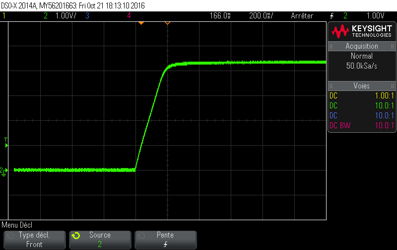
Then, I switch on the input voltage (390 Vdc). LM25037 is supplied with 10V on pin VCC and VIN.... The UVLO is OK. The Soft-Start is also OK : rises to around 5V. But I can't see any ramp signal on the RAMP pin !! It looks like the oscillator of the LM25037 does not operate...

The values for RT1 is 14k7 and for RT2 is 20k (around 400 kHz clock and 200 nsec dead-time to limit the duty cycle to 88% roughly...). A voltage appears on these resistors too....

So, what's going on and why the LM25037 does not oscillate ?

By the way, the current sensing is done with a shunt, and then a 2nd order Sallen-Key activ Filter. So, the CS pin is directly connected to the output of a OpAmp.... and then connected to RAMP through a capactor to get the slope compensation. RAMP is connected on 10V through a resistor....

Could you please help me ?

Thanks a lot,

Cheers,

Julien.

  • Julian,

    Can you post your schematic so we can review it in detail?


    Thanks,
    Bernard
  • Hi Bernard,
    the schematic is confidential... I can sketch how the controller is implemented if it can help you...
  • Julien

    If you could post at least the connections to the pins of the LM25037 with R & C values, that would be helpful.

    Alternatively, you can send me the schematic, partial schematic, or sketch to my email: bernardkeogh@ti.com

    Thanks,
    Bernard
  • i will do it for sure.... :-)
  • Hi,

    here is a screen shot of the implementation of the LM25037.

    The voltage applied on R9 is from 370V to 410V I do my test with 390V. UVLO is ok because soft start goes hi too…

    Switching frequency is around 216 kHz. (CLK = 432 kHz)

    Thanks in advance for your precious help !

    Greetings,

    Julien.

  • The OpAmp are Rail-to-Rail type.

    Here are the voltages I measured :

    RT1 = RT2 = 2V

    CS = 0V

    RAMP = 0V -> I have no ramp, no pulses !! it remains to = OV

    UVLO = 1.56V

    COMP = 0V

    FB = 5V.... is it coming from that ?

    But I get no pulses during Soft-Start ? This voltage rise to 4.5V clearly when UVLO is above 1.25V....

    Thanks for you precious help...

  • Julien,

    I think there are a few issues.

    Firstly, I think your issue is maybe complicated by the op-amp filter driving the CS pin. I am curious why you need to use an active filter for the CS signal? Typically a simple RC filter is usually sufficient.

    Secondly, the RAMP pin components look like 819 k-ohm and 1.5 nF, which is very long time constant of 1.23 ms, compared to the osc period of 2.5 us. This could also be the issue, this will set up an very low amplitude RAMP ~ 20 mV peak at the end of the 2.5-us osc period.

    I would recommend setting up the LM25037 CS & RAMP pins as shown in the datasheet page 18/19, using eqn’s 4-6 to calculate the required component values. The normal CS ramp appears should appear across the CS pin filter cap, and then the extra cap between CS & RAMP allows the slope comp ramp to be summed.

    Initially, I would suggest setting the RAMP pull-up resistor appropriately. If the circuit is still not working, then try removing the op-amp filter cct on CS pin, and use a simple R-C filter, to see if that helps.


    Thirdly, if the FB pin levle is 5 V, this is well above the internal error amp ref level of 1.25 V, so this will drive COMP low to 0 V as you observe, and regardless of everything else above, this will prevent any PWM pulses being generated. I would suggest that you double-check the polarity of the external error amp being used. Or is there another op-amp active filter driving the FB pin? I would recommend using a simple resistor-divider on the output voltage to feed the FB pin.


    I hope this information is helpful.


    Thanks,
    Bernard
  • Hi Bernard,

    thank you very much for your kind help.
    I am using current mode control and designed the CS, and RAMP refered to the datasheet. I have a very small current and a very low output ripple... The primary current is 0,7 A max. I use active filter because the controller is far away from the power section... I want a very clean signal too....
    I used an active filter too after my optocoupler to sense the output voltage...

    I will check one more time the values Cslope and Rslope and modifiy my output voltage sense, so that it sees 0V instead of 5V when the output voltage is 0V....

    I keep you in touch then.

  • Hello Bernard,

    So, I have made some modifications and the LM25027 start and generated PWM.

    Slope Compensation ramp is yet around 50 mV and the PWM engine could start.

    the FB voltage is around 600 mV for 0V output voltage and I built a new circuit, so that it sees 1,25V when the output voltage is 350V.

    The problem is that I did not see a low duty cycle during soft-start. I triggered one PWM output and the duty cycle is 90% for the first pulses…

    By the way, i tried to start the full-bridge with the power section, but when it started to pulses, the Mosfet cracked and the bridge gone out of order… There were no short-circuit as the hi voltage source did not come into current limitation…

    I noticed that the PWM outputs of the LM25037 were out of order too… (the controller sinked 0,12 A supply current…)

    So, my questions are :

    1. Why I do not see low duty cycles pulses at soft start ? The soft-start ramp is increasing to 1V and then 4,5V as predicted, but the pulses remain 90% duty cycle. Dead time is 150 nsec and switching frequency is 200 kHz (CLK = 400 kHz)

    2. Do you think it could come from the layout ? I plugged the PWM output of the controller direct to the input of the half-bridge PWM driver.

    Thanks in advanced

  • Julien,

    You will need to show the details of the schematic and value changes you made, otherwise it will be difficult to figure out what is happening. Also waveforms of the RAMP, COMP, SS, CS, OUTA/B pins would be useful.


    Going back to your previous posts, I think even if the controller is some distance away from the power stage, it should not be necessary to use an active filter for the CS signal. Even if the current is relatively low (0.7 A), you can generate the required signal using the right Rcs shunt value. And since the CS pin fault protection level is quite low (0.255 V), the shunt power dissipation will still be very small, even without an amplifier. The RC filter at the CS pin should be located close to the CS pin of the LM25037 - the line from the Rcs shunt is very low impedance, so it's a lot less susceptible to noise pick-up.

    For the feedback loop, you earlier said:
    "The image of the output voltage is transmitted through an opto-coupler and then a PID controller is directly implemented between the transistor of the opto-coupler and the FB / COMP pin of the LM25037."

    For isolated outputs, the LM25037 internal error-amp is typically bypassed and not used. This is because it's not possible to transmit the absolute output voltage level through the opto-coupler, due to the CTR variability. Typically, the error amp and PID compensation are all placed on the isolated secondary side, and then an error or demand level signal is coupled to the primary through the opto-coupler. This way, as the CTR of the opto varies (from unit to unit and over temperature/life of each unit), the error amp will adjust it's output level to compensate, to get the required demand level at the COMP pin to get the right duty cycle for regulation. As shown in the schematic on page 1 of the datasheet, with isolated outputs, the FB pin is tied to GND on the primary side, the COMP pin level will then internally try to pull up to max level, and the opto will pull-down COMP to the right level for regulation, driven by the secondary-side error amp (typically TL431 or similar).

    For non-isolated applications, the LM25037 internal error-amp is normally used, the output voltage can be resistively divided and connected directly to the FB pin, and then the loop compensation components are placed between FB and COMP, as shown in the design example at the end of the datasheet.


    For initial open-loop testing, you can leave the FB pin connected to GND, disconnect the opto feedback, and then put a variable resistor (potentiometer) from COMP to GND. Since the COMP has an internal pull-up of ~5 k to the internal 5-V ref, the COMP can be pulled close to GND by pulling ~1 mA current out of the pin to GND. This test setup will allow you to slowly increase the COMP level, and see the gate pulses you get. Because of the 1-V internal offset from COMP to RAMP comparator, there will be no gate pulses until the COMP level has reached ~1 V, then the pulses should start with small duty cycle. As COMP is increased further, the duty cycle will increase. The rate of increase depends on the slope of the PWM ramp at the RAMP pin. Also, the Dmax duty cycle of ~50% on each output will be reached at a COMP level which depends on the RAMP pin slope. If the RAMP slope is very shallow, Dmax will be reached at a lower level on COMP. If the RAMP slope is very steep, then the duty cycle may not reach Dmax, even with COMP at the max level of 5 V.

    For initial testing, I would also suggest not using any current-mode CS signal, just use a voltage-mode ramp open-loop to command the required duty cycle to see that OUTA/B are driving the bridge-stage correctly with open-loop user-controlled duty cycle.

    For your most recent questions - after initial startup, the SS cap is charged through a 100-uA internal current source. During soft-start, COMP is forced to follow the SS pin, until the COMP level reaches its required regulation level - during soft-start, the SS can internally pull-down on COMP to force the 2 voltages to track, but SS cannot drive COMP higher than the level it settles at based on the external pull-down.

    In your case, you use 3.3-uF SS cap, so it will charge up by ~300 mV in every 10 ms. Until SS gets to 1 V (i.e. COMP also ramping to 1 V), there will be no PWM, so for the initial 33 ms of SS, there will be no PWM. At 1 V PWM will commence, and the rate of PWM duty cycle increase depends on the RAMP slope. If your RAMP is only 50 mV, the duty cycle will immediately go out close to the 50% Dmax. In this case, you are relying on getting a large enough CS ramp component to terminate the PWM, but it does not seem to be doing that. If you test without the power stage, there will be no CS signal, since no current will flow. But there may also be an issue with the CS signal generation, it may not be generated, or it may be too small. I would recommend to initially test in voltage-mode, with a large RAMP amplitude, and control the COMP level open-loop as explained above, to get fixed user-controlled duty cycle - this can be used to ensure that all the parts of the circuit are working correctly, including the CS ramp generation.


    Thanks,
    Bernard
  • Dear Bernard,

    thank your so very much for detailed explanation of how the LM25037 internally really works, especially how RAMP is built in…
    I though that RAMP was only here to provide a slope compensation for current mode control and that the LM25037 generated an other internally RAMP for the PWM modulator… In the datasheet, this is not really well explained and detailed… So, the RAMP should be large enough to get the full duty cycle range from 0V to 5V (max. COMP voltage…) but small enough to bring an additional slope compensation ???…… it sounds strange… I think I will use this controller in voltage mode and use an external current protection…

    I use a linear optocoupler to sense the output voltage because I do not want to have to generate an additional VCC_supply on the secondary side to supply OpAmp and REF like ATL432 (which is really good + OPA171 which is also very nice… works very nice for my HV discret linear regulator !!). and the LM25037 incorporates an OpAmp…
    By the way, I will test the power section of my board in open loop and keep you in touch…

    Have a nice day and thank you vey much for your kind help.
  • Julien,

    The LM25037 is flexible and can be used in several modes, since the RAMP pin is just the input to the internal PWM comparator, several different external ramp sources or a combination can be connected to that pin:

    - voltage-mode with fixed PWM ramp, with RAMP pull-up resistor to fixed DC rail (e.g. REF pin) - working COMP range 1.2-4.5 V.

    - voltage-mode with feedforward PWM ramp, here the RAMP pull-up resistor is connected to VIN - working COMP range 1.2-4.5 V. In this mode, the ramp slope increases with higher Vin, so even without any feedback control action, this gives natural Vin feedforward, the duty cycle changes automatically inversely proportional to Vin regardless of feedback. E.g. at a certain Vin and load, the COMP will sit at a certain level, and will produce a certain duty cycle D. If Vin is doubled, the RAMP slope will double, so even before the control loop can move the COMP level, the RAMP will intersect COMP in half the time (2x slope), so the duty cycle goes to D/2 even before the feedback loop reacts. This is explined in detail in sections 7.4.1 and 8.1.2 of the datasheet. This works well and is often used when current mode is not required or is difficult (very high current etc), and allows for a large amplitude pk-pk RAMP signal.

    - peak current-mode, with only the CS shunt signal used to generate the PWM ramp - this is what's shown in the simplified sch on page 1 - the CS and RAMP pins are shorted together, and there is not other input to RAMP - just the CS shunt signal. In this case, since the CS internal protection comparator has a trip level 0.22 V min, the power stage and Rcs shunt must be designed for full-load full scle < 0.22 V - so this restricts the working range on COMP to 1.2-1.42 V. In practice, since slope comp is almost always needed, the IC is rarely used in this mode.

    - peak current-mode with slope comp - as shown in sections 7.4.2 and 8.1.3 of the datasheet. This combines the 0.22-V max CS signal with some portion of v-mode ramp for slope comp for stability in CCM with D>25% per phase. Again, the RAMP working dynamic range is quite small in this mode, since CS is limited to 0.22-V max. A larger CS signal could also be used with a larger Rcs shunt for better noise immunity, and the Rcs signal could be scaled down at the CS pin to adhere to the 0.22-V limit.


    As you say, FFWD V-mode may be a better option for you in this application, and should ebeasier to debug initially.


    Thanks,
    Bernard
  • Thanks again for the details. I have now a better understanding.
    I originally designed the full bridge in voltage mode but switched to current mode because I wanted to avoid a non balancing current load in the primary of the transformer…

    Tell if I am wrong : I will try to increase the slope of the RAMP pin to get for instance 1.2V max at the peak of the ramp.
    I will try in voltage mode, and then in current mode by connecting CS to the bottom of the cap of RAMP to see if there is a difference about the regulation…

    One question : why is there always a 1V offset at the input of PWM comparator ? Is this for noise immunity ?
  • Dear Bernard,

    I have done further measurements.

    I increased the RAMP to 2V.

    Soft-start is working good.

    And now, I have no PWM pulses during soft-start anymore… The voltage at COMP pin remains 0V during the whole soft start process…

    Power stage is disconnected and there is NO current sense signal at CS pin… So, I am in voltage mode…

    By the way, during my first experiment, I had up to 10V on the FB. the recommended max voltage is 7V… do you think the FB/COMP bloc is dead ?

    VOLTAGE FB PIN

    RAMP

    SOFT START

  • Julien,

    First of all, the purpose of the offset from COMP to RAMP is so that COMP can be pulled low to command zero duty cycle, but it only needs to be pulled to ~1 V typ to get 0%, this makes the pull-down much easier since it does not need to go all the way to GND, and can be pulled down through a diode etc. The standard UC284x architecture uses a similar internal offset.

    If you see COMP held low while SS rises, then something external must pulling and holding COMP low, or less something external is pushing FB high, above the internal REF, which will then force COMP low. Remember that the SS buffer can only pull down on COMP internally to force SS & COMP to track, but it cannot drive COMP higher than the level COMP wants to be at - this makes COMP & SS track only until the required COMP level is reached - which could be zero, depending on what;s externally driving FB or COMP.

    The CS pin is also NOT used at all for PWM or current-mode control, ONLY for over-current protection. It's good practice to continue to connect your current-sense signal to CS (assuming it's working and properly scaled), so that the CS pin can give some over-current protection if required. Look at the overall IC block diagram on page 9.

    Current-mode signal (if used) is coupled to the RAMP pin.


    I think if the FB pin was raised to 10 V at some stage, it's probably unlikely to be damaged. However, if the IC is misbehaving, even if it's down to a system or usage issue, it may be wise to use a new IC anyway, just to factor out the possibility of damage.


    Thanks,
    Bernard
  • Dear Bernard,

    The controller is working fine and I can control the duty cycle with the COMP voltage. Thanks for all your advise.
    The full bridge is OK too. I have some oscillations when the Mosfets turn off, but I think this is due to the fact that the primary current is in discontinuous mode.

    I thought to an other solution for the control scheme : what is your opinion about the implementation of the controller on the secondary side to have a better time response for the regulation, and then drive the Mosfet throught opto-couplers ??

    Cheers Julien.
  • Julien,

    I am glad to hear that you have resolved your issues and your circuit is now working.

    If you want to move the controller to the secondary side, you could drive the primary MOSFET's using some of TI's isolated gated rivers. E.g. UCC21520 or UCC21521. These are fully safety agency approved and provide high-speed isolated gate drive with low prop delay.

    You would need to add a low power bias supply to the system, to generate a primary-referenced VDDA/VDDB rail for the driver, and an isolated secondary bias rail for the LM25037 to get things started up, and to power the secondary side of the driver VCCI. But you may already have such a bias supply since you already generate an external +10V supply on the primary side.


    Thanks,
    Bernard
  • Dear Bernard, 

    I have some further progress. 

    I replace the opto-coupler by an isolated Op-Amp from AD (ADuM3190), and place the PID controller own the secondary side.

    Here you can see some measurement.

    My main problem, is that the duty cycle is not constant and oscillating… causing some voltage imbalance on the primary of the transformer…

    The switching wave-form are clean and the oscillations when the Mosfet switch off are, I think due to measurement error and parasitic effects of the probes… The Probes are directly solder on the pins of the primary winding…

    I think I have a good PID regulator, because the soft-stat does not oscillate anymore… 

    So, my question is : where do you think come this little instability… The output voltage is, by the way, really constant.

    Please, not that I am at that moment testing at only 120V input voltage instead of 390V … I am increasing to full load nicely… Want to be sure that everything is stabil… I have 4 secondary windings and only 1 is used for feedback… The output voltage that I measure, is took on one of the windings that is not regulate…

  • BLUE + GREEN = Lower Mosfet Vds.
    PINK = Primary Voltage