This thread has been locked.

If you have a related question, please click the "Ask a related question" button in the top right corner. The newly created question will be automatically linked to this question.

UCC28070: Active power factor correction

Part Number: UCC28070
Other Parts Discussed in Thread: UCC28063

Hello,

I am using UCC28070 interleaved PFC controller for 1.2kW battery charger design. I have few queries regarding this IC. These are mentioned below.

1. Does duty cycle in boost PFC varies according to input sine voltage? 

2. What are the advantages and disadvantages if we keep duty cycle constant?

3.  What are the advantages and disadvantages if we keep duty cycle variable?

4. Why loop bandwidth of PFC is always kept low such as at 20Hz?

Regards,

Dhananjay

  • Hello Dhananjay,
    I will answer your questions in the order you wrote them:
    1. The UCC28070 is a CCM type pfc controller and the duty cycle varies with the instantaneous value of the input voltage.
    2. The UCC28070 cannot be used with a fixed duty cycle. You can use the UCC28063 transition mode controller in this way but 1.2kW is beyond the power handling range of this controller. The peak currents are simply too high and the power losses great.
    3. The advantage of variable duty cycle is that the current can be forced to accurately track the voltage and achieve good power factor.
    I can think of no disadvantage
    4. The loop bandwidth is is usually set at about 0ne tenth of the minimum rectified input frequency. This is so that the loop does not attempt to track each cycle of the input voltage but rather the average value.

    Regards,
    John
  • Hello,

    Thanks for the quick response.
    If the loop bandwidth is one tenth of rectified input frequency, then how does the duty cycle vary at input frequency?
    Thanks
  • Hello John,

    Can you please answer to above query?
    Regards,
    Dhananjay
  • Hello Dhananjay

    John is travelling at present and his responses may be delayed.

    In the meanwhile - I'd suggest you look at the material on PFC at http://www.ti.com/ww/en/power-training/login.shtml?DCMP=psdslibrary&HQS=tlead-power-psdslibrary-apec2015-pwrhouse-20150312-lp-en      The article at https://www.ti.com/seclit/ml/slup203/slup203.pdf is a good introduction to PFC in general.

    Overall, the slow loop response (typ 10 Hz or so) allows the controller to set an AVERAGE current level in the PFC inductor which is then modulated (or multiplied) by the instantaneous input voltage (a sinusoid). You can see the MULT block in the UCC28070 data sheet block diagram. This modulation is what modified the duty cycle as the line voltage goes through it's cycle. This way you get a sinusoidal input current whose AVERAGE level is correct for the load conditions at the output.  there are some subtlties of course but that's the basic idea.

    Regards

    Colin

  • Hello,

    What is the minimum duty cycle that UCC28070 can offer?

    Regards,
    Dhananjay Yadav
  • Hello Dhananjay

    The minimum duty cycle is zero.

    Regards

    John

  • Hello John,

    Thanks for reply!
    Please let me know at maximum instantaneous input AC voltage duty cycle will be minimum or maximum? 

    And at zero instantaneous AC input voltage what will be duty cycle value?

    Regards,
    Dhananjay Yadav

  • Hello Dhananjay
    Equation 42 in the datasheet shows how D varies with the input voltage.
    You can see that the peak value of Vin corresponds with the min value of D and the min value of Vin corresponds with the max value D

    Regards
    John
  • Hello John,
    Thanks for reply!
    But I am not able to realize this concept. This is for the 1.2 KW battery charger PFC stage.
    Can you please tell me is duty cycle is in phase with input AC wave or it is out of phase?
    Please find below image for reference. Is it like the same as shown?

    Dhananjay Yadav

  • Yes the duty cycle waveform looks like it is behaving properly.
  • Hello John,

    What is typical bandwidth of current loop and voltage loop?

    Regards,
    Dhananjay Yadav
  •  Hello John,

    Thanks for reply.
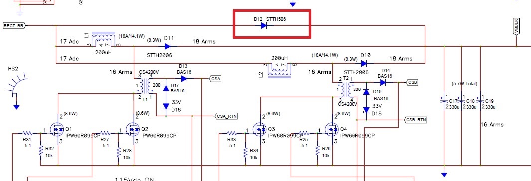
    Can you please let us know the use of the boost bypass diode as highlighted in attached image.
    Our input ac rms voltage range is 165 to 295 and o/p of PFC is 420V . So please let us know the use case of boos bypass diode in our application?

    Regards,
    Dhananjay Yadav

  • Hello Can you please reply to above query?
  • Hello Dhananjay

    The purpose of the bypass diode is to carry the initial inrush currents when the PSU is first connected to the line. The output capacitor will have 0V across it and will rapidly charge to the peak of line - this happens before the PFC controller starts. If this bypass diode is not fitted, then this current will flow through the PFC inductor and PFC diode but the problem is that the Fast diodes used for the PFC output diode don't normally have a high enough surge current rating - the parallel bypass diode keeps theese surge currents away from the PFC diode. It has no other function and is inactive during normal operation of the PFC stage. You can evaluate the surge currents in your own design and remove the bypass diode if your PFC diode can carry them - but be careful because this is not normally the case.

    Regards
    Colin
  •  Hello,

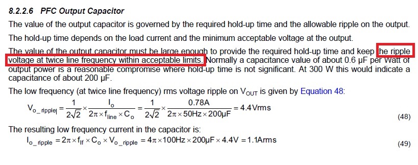
    1. Below screenshot is from datasheet of UCC28070 (Page no: 32). Please see highlighted box in red color. Can you please let us know why output capacitor is considered at twice the line frequency?

    2. Is Protection from undervoltage and overvoltage on AC input line is available on UCC28070?   

    Regards,
    Dhananjay

  • Hello Dhananjay
    The answer to your first question is it will be minimum and to your second question it will be whatever maximum value is set on the DMAX pin.

    Regards
    John
  • Sorry I was looking at an earlier question.
    The output ripple frequency is at twice the line voltage because of the bridge rectifier. This sets the low frequency output to twice the line.
    There is no protection from input overvoltage on the UCC28070.
    It does not have a brownout protection but at low line input the UCC28070 goes into current limit and the output voltage drops. Also the maximum duty cycle limit is reached which further tends to decrease VOUT.
    The UCC28070 turns off when VSENSE drops below its undervoltage limit

    Regards
    John
  •  Hello,

    1. Regarding low AC input voltage: It is understood that Vout will decrease as 28070 will go into current limit and duty cycle limit also reaches. But I could not find the value in datasheet at VSENSE pin where UCC28070 turns off. Please guide.

    2. If Under voltage protection is already present, then why it is added externally in TI's one of the reference design? Please refer to below image.(File: PMP4311A_Sch_RevA.sch)

    3. As there is no protection from over voltage , so we need to add external circuitry for this right?

    4. But in case of overvoltage, where VINAC peak value > VPFC output, 28070 will reduce duty cycle(28070 will go into voltage limit cycle) and at certain AC input over voltage it will become zero right?

    Regards,
    Dhananjay Yadav

  • (1) Look in the data sheet for the section on "pfc enable".
    This value is 0.75V
    (2) Under voltage naturally occurs when the value of VSENSE <0.75 and then PWM ceases.
    If a brownout voltage needs to be set independently of VSENSE then an external circuit is needed.
    (3) This is totally dependent on your design requirements.
    (4) The UCC28070 stops PWM when the output voltage reaches 106% of the nominal set point

    John Griffin
  •   Hello John,

    Thanks.

    We have another query. In ZVT section, a resistor and capacitor is placed in series with gate drive transformer primary coil winding. Can you please let me know the reason behind this? And how to select these resistor capacitor values.

    When we are simulating below circuit, the waveform is settling after 300usec approx. Considerinf 200KHz switching frequency, will there be a problem? Please guide in selecting cap and resistor value.

    Regards,
    Dhananjay Yadav

  • Hello,

    Can you please reply to this?

    Regards,
    Dhananjay
  • Hi Dhananjay

    1. Does duty cycle in boost PFC varies according to input sine voltage?  

    A:Yes. the basic relationship is D = 1 - (Vin/Vout) - Vin varies sinusoidally so D must vary too.

    2. What are the advantages and disadvantages if we keep duty cycle constant?

    A: you cannot keep D constant because of the relationship above

    3.  What are the advantages and disadvantages if we keep duty cycle variable?

    A: A variable D allows you to control thn inductor current to be sinusoidal

    4. Why loop bandwidth of PFC is always kept low such as at 20Hz?

    A: The input power varies sinusoidally (due to the rectification) at twice line frequency but the load power taken from the output is constant. This means that there is a sinusoidally varying difference between the power going into the output of the boost converter and that being taken off it. The result is a sinusoidal variation in the output votlage of the Boost. This variation is normally 'small' in relation to the DC average voltage  - about 20V pp on a 400V output is typical. The problem is that the control loop must be prevented from reacting to this sinusoidal variation at 100Hz or 120Hz and the normal way to do this is to have a very low bandwidth - normally it will be in the range 7Hz to 10Hz

    You will find more information on PFC and other topics at http://www.ti.com/ww/en/power-training/login.shtml?DCMP=psdslibrary&HQS=tlead-power-psdslibrary-apec2015-pwrhouse-20150312-lp-en

    Regards

    Colin

  •  Hello,

    Thanks.

    We have another query. In ZVT section, a resistor and capacitor is placed in series with gate drive transformer primary coil winding. Can you please let me know the reason behind this? And how to select these resistor capacitor values.

    When we are simulating below circuit, the waveform is settling after 300usec approx. Considerinf 200KHz switching frequency, will there be a problem? Please guide in selecting cap and resistor value.

    Regards,
    Dhananjay Yadav

  • Hello Dhananjay

    I can't find the ZVT section you mention - please send me a link to it.

    Regards
    Colin

  • Hello Colin,

    Please find below file. In this file please check gate drive transformer circuit. (Page no: 4)

    Regards,
    Dhananjaysluu421a.pdf

  • Hello Dhananjay

    The capacitor is present to prevent a DC bias current flowing in the gate drive transformer primary. A DC current can saturate the transformer and make it ineffective. The resistor is there to limit the peak current as the MOSFETs are switched.

    If you design the transformer to accept a small DC bias then the capacitor is not needed. The main criterion for the capacitor is that the voltage across it does not change too much (let's say about 10%) during the switching cycles.

    Regards
    Colin