This thread has been locked.

If you have a related question, please click the "Ask a related question" button in the top right corner. The newly created question will be automatically linked to this question.

UCC27531: UCC27531DBV

Part Number: UCC27531

Hello E2E support team,

Currently in one of my design I am using UCC27531DBV mosfet driver for switching 24V supply to load.

As per truth table mention for the device, when EN and IN both pins are active LOW, OUTH shall be High Impedance state, however I found OUTH value as 7.5V.

With this my P-channel mosfet gets turned ON, however it shall not be turned on???

Below is the snap shot of the circuit diagram:

When both IN and EN pins are low, how much voltage we can expect at the OUTH pin?

When PS_EN signal is driven LOW, T12 mosfet is switched OFF, so T1 should be also OFF.

When PS_En signal is driven HIGH, and IN is still LOW, as per truth table we shall get High Impedance at the OUTH pin, but in that case alsoT1 is turned ON.

However when both IN and EN pins are driven HIGH, T1 mosfet is switched OFF - that is correct as per the truth table - and designed to work in that way.

Please explain this behaviour of the UCC27531DBV?

Best Regards,

Rajesh

  • Hi Rajesh,

    Thanks for considering TI part for your design and I will try to help you resolve this issue.

    Did you measure 7.5V at DRVH pin of UCC27531 after removing R11 to make sure that the leakage voltage is coming through the driver and not through R8, R74, and T12 parasitics?

    As the output is high impedance, if there is leakage voltage through R8, R74, and T12, then I believe T1 will be turned ON as the gate voltage is going to be lower than the source voltage for PMOS.

    As you mentioned, when both EN and IN is high, the DRVH goes to almost VDD value and that way the gate of PMOS is higher than source and therefore, the PMOS turns OFF.

    Please let me know your findings. Meanwhile I will check with our design team to see if there is any internal leakage part or it is just output capacitance of the pull-up FET inside the driver.

    Regards,

    Ritesh

  • Hi Ritesh,

    Thanks for quick reply.

    I removed R11 and measured voltage at DRVH pin, it is about 2V, and T1 doesn't get turned ON (its gate is at 24V, showing that there is no leakage through R74 & T12)

    When R11 is mounted and R74 is removed to isolate T12, I found that OUTH pin is at 7.5V.

    What surprised me is that there is no change in this voltage at OUTH pin even when R74 is mounted and whether T12 is ON (I verified T12 drain to be 0V) or OFF (T12 drain was verified to be 7.5V itself, showing that there is no loading by T12 when it is OFF).

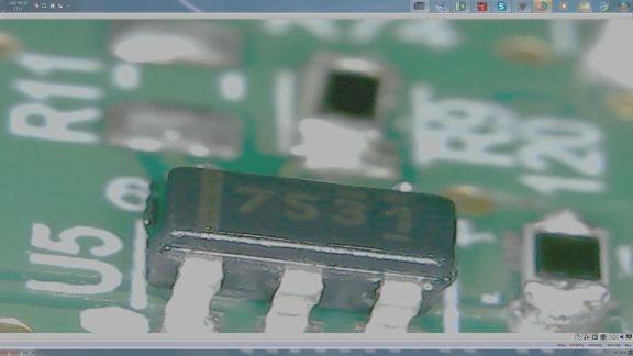
    I also verified top marking for the assembled part to be 7531, see the attached image.
    Did you check internally on this issue?

    Do you require any other info, please let me know?

    Best Regards,

    Rajesh

  • Hi Rajesh,

    Thanks for providing those test results.

    I believe there is an impedance network formed by R8, R11, R74, parasitic impedances of T1 and T12, and driver internal impedances from VDD to OUTH as well as OUTH to GND.

    I have asked my design team to take a look, but it might take some time before they would come back to me.

    Meanwhile, you can see the effect of voltage when you change the value of those impedances that can be controlled, i.e. R8, R9, R11, R74, R142, CK4

    Regards,

    Ritesh 

  • Hi Rajesh,
    I discussed this issue with our design team and found out that the driver has internal 7V Zener at the gate of the pull-up NMOS shown in the datasheet page 20. This zener is required to protect the gate oxide when the voltage exceed 7V.
    I believe you can attain the functionality you are trying to attain if you tie OUTH and OUTL together and connect them to R142. Of course remove R11. This way, when T12 is ON, the load switch would be ON and when T12 is OFF, the load switch would be OFF.
    Please let me know, how else I could help.
    Regards,
    Ritesh