This thread has been locked.

If you have a related question, please click the "Ask a related question" button in the top right corner. The newly created question will be automatically linked to this question.

UC3845: Driver circuit

Part Number: UC3845

I am working on a dual switch flybck converter using UC3845.

To drive two MOSFETs, a driving transformer is used. The driving circuit is shown in fig.1.

The primary side is a DC blocking capacitor which is 1uF. The secondary side is driving resistor which is 15Ohms.


fig 1 driving circuit

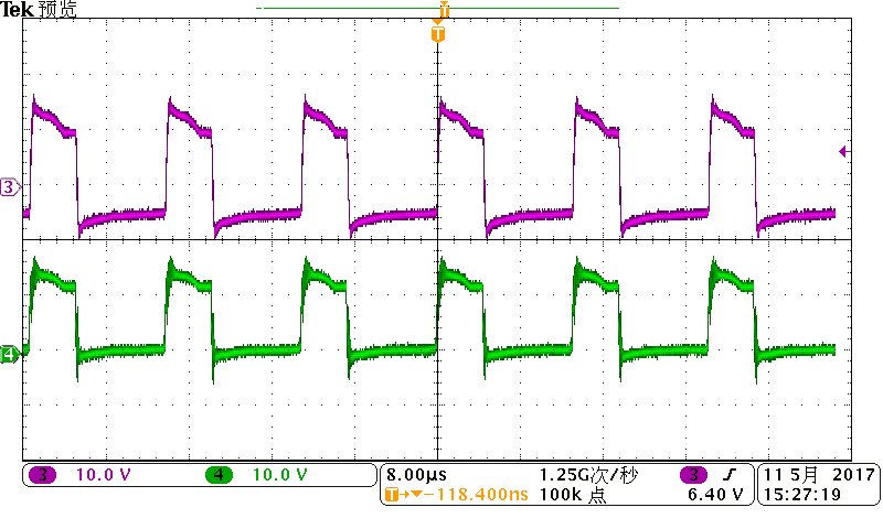
Here comes the question. The output of UC3845 pin6 is shown in channel 4 in fig.2, which is a little weird. Channel 3 is voltage across GS of MOSFET.

When the switch is on ,the voitage is not as constant as supply voltage about 14V. There is a descending ramp.

I cannot figure out why...It looks like something wrong with the IC UC3845. However if I take the DC blocking cap. The output of pin 6 is OK.

fig.2

  • Fumin,

    What is the magnetising inductance of the gate drive transformer? I assume the turns ratios are all 1:1:1?

    The DC-blocking capacitor is required to AC-couple the OUT waveform, so that the primary of the gate drive transformer sees equal positive and negative volt-seconds to keep it balanced. If VCC = 15 V, and OUT high ~ 15 V, then at 50% duty cycle, the primary will see +/-7.5 V, and the blocking cap will have ~7.5 V across it with some ripple. So at this operating point, assuming 1:1 turns ratio, the MOSFET gate will also be at ~+/-7.5 V levels

    Depending on the blocking cap value, the transformer mag inductance and winding resistance, there will be some ripple, due to the cap ripple voltage and the I*R drops on the winding resistance and the internal resistance inside the OUT pin. If the magnetising inductance is too small, the pk-pk magnetising current will be large, and the IR drops will be large, and maybe the current could be so big to cause the OUT pin voltage to sag.

    If you put the blocking cap on the GND side of the primary, you can observe the voltage across the cap to see the ripple. You can then observe both OUT pin and cap voltage, and subtract (using scope math function) to see the voltage across the primary.

    Basically, sue to finite cap value and finite magnetising inductance and non-zero resistance, there will always be some ripple on the MOSFET gate. As long as the ripple is acceptable to keep the MOSFET safely turned on, everything should be ok.


    I hope this answers your question, if so, please click the "verify answer" button.

    Thanks,
    Bernard
  • Thank u! i am sorry to be so late to reply u. I didnt receive notification until today when i opened computer and logined the forum again. i dont know why...

    The point of your answer is that due to the finite magnetising inductance and capacitance , the magnetising current may be a little big which may cause some voltage drop across the winding resistor and inner reisitor inside the OUT pin. Am I right?

    The primary inductance is 330uH,the secondary inductance is 577and 574uH , the turns ratio is about 1:1.3:1.3. Is that magnetising inductance too small?

    since the transformer is boosting voltage, current in primary winding is bigger, and the driving transformer needs to drive 2 mosfets. Is there any possobility that the driving current of UC3845 is not enough?
  • Fumin,

    Yes there will be ripple due to the pk-pk magnetising current flowing in the internal resistance of the OUT pin plus the transformer primary resistance, and also some voltage ripple across the DC-blocking cap.

    If the magnetising inductance is 330 uH, for approx.. 5 us on-time as shown above, with 14 V VCC, that's about 200 mA pk-pk.

    The OUT pin drive resistance is ~5-10 ohms, so that's about 1-2 V pk-pk ripple.

    Similarly, for 1 uF cap, the ripple voltage will be ~1 V pk-pk (maybe more due to decrease of the effective cap value with applied DC bias).

    As I said above, the magnetising inductance will always be a finite value, there will always be some magnetising current, so there will always be some ripple on the gate drive - the design just needs to ensure that the ripple is tolerable wrt FET Vgs(th) and Rds(on).

    If this answers your question, please click the "verify answer" button.

    Thanks,
    Bernard