This thread has been locked.

If you have a related question, please click the "Ask a related question" button in the top right corner. The newly created question will be automatically linked to this question.

UCC28630: No voltage appears and the secondary side of the transformer and also all the pins of the UCC28630 just except for the HV pin.

Part Number: UCC28630

Hi, all.

I have a problem about my SMPS circuit with the UCC28630 that no voltage appears at secondary side of transformer.

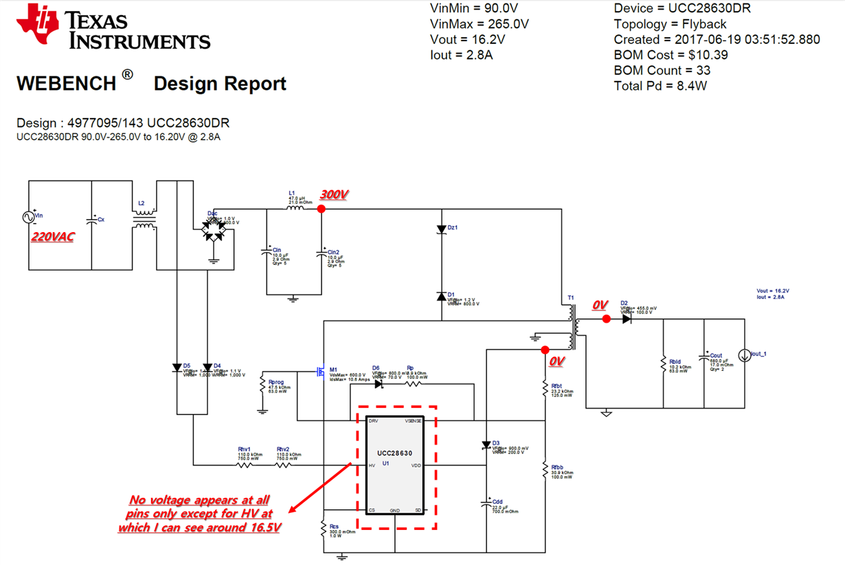
I've checked the circuit, and found no voltage appears as well at all pins of the UCC28630 except for the HV pin at which I can see around 16.5V. I've tried to debug where this failure comes from, but failed. Could you let me know if you have any good idea to solve this problem?

For your reference,

  1. I used the WEBENCH design tool to design the SMPS, and the attached diagram is the one I got from the tool. I've made my SMPS circuit exactly same as this diagram.
  2. I've also checked the power transistor, M1 separately, and it's OK. It works and was destroyed.
  3. There was a sequence of events to failure.
    1. At first, as we saw no voltage appears at the secondary side of the transformer, we found D1 was mounted reversely. Then we corrected it, however the SMPS still doesn't work. I'm not sure if this incorrect mounting of D1 could permanently damage on some components in the circuits.
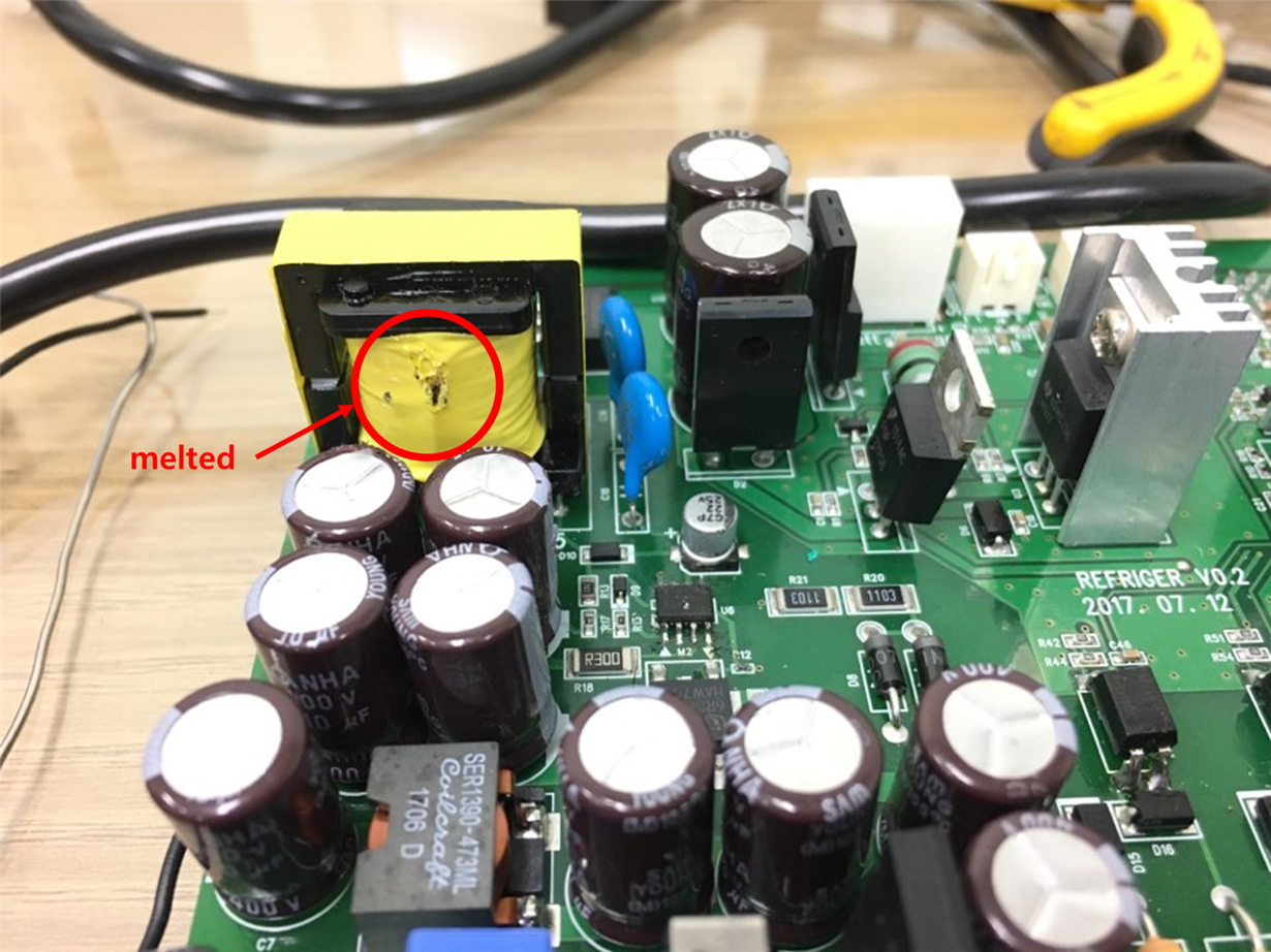
    2. second,  after repairing D1 position, we found also a surface of the transformer was melted partially as you can see in attached picture, so I wonder where this comes from, and if it could be an symptom of the failure.

Thanks in advance!!

  • Hi Kyutae,

    Thank you for reaching us again on E2E. The easiest way to fix the circuit is to replace the new transformer, MOSFET, UCC28630 controller, and the freewheel diode (D1), and see if the problem persists.

    The possible cause of failure is due to the freewheeling diode D1 was reversely populated as you mentioned. There was no free-wheeling path for the inductor current when the FET was turned-off (OPEN) during the first switching cycle. This induced a very large voltage spike on the switching node due to high di/dt of the inductor current and further damaged the FET and X'FMR and perhaps of the controller IC. For further information on how does a flyback free-wheeling diode work, please refer to this article: https://www.elprocus.com/freewheeling-or-flyback-diode-circuit-working-functions/

    I hope this would help to clarify your question, and please let me know again if the problem still persists after the components are replaced.

    Thank you.

    Best Regards,

    Wei-Hao Chen

  • Hi Wei-Hao.

    Thanks for your always kind help!!

    I will try to replace the components you commented.

    Additionally, could you let me know how I can check if the UCC28630 is destroyed and any faults in the UCC28630?

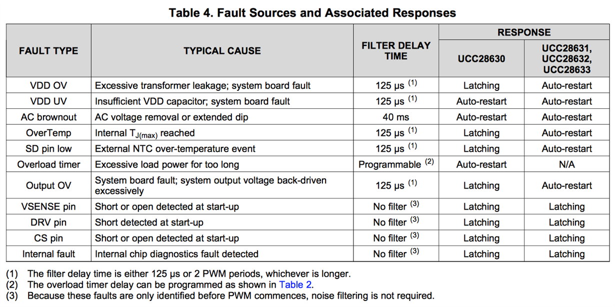
    I read the datasheet about fault mode as attached table below, I'm not sure how I can use it as I check the pin of the UCC28630.

    Thanks!

  • Hi Kyutae,

    The fault response table refers to the protection action the controller would take if the given fault condition occurs. Latching means the IC will stop any output completely until the IC is reset; whereas auto-restart refers to the IC will shut down for the amount of time and automatically re-attempt to check if the fault condition still persists.  

    But you cannot use this table to check if the IC is damaged or not. You may check the impedance of the pins to compare with the new device. Or I would suggest you get a UCC28630 evaluation board to see the behaviour of the controller and compare with your board. The information of the evaluation board is in the link below:


    Thank you.

    Best Regards,

    Wei-Hao

  • Thanks Wei-Hao!
    I have one more question about "auto-restart".
    If fault conditions were not solved, does the IC keep shut-down of the pins of VDD UV and AC brownout? And if UCC28630 was not destroyed, does the IC keep the action of auto-restart repeatedly?
  • Hi, Wei-Hao.

    I've replaced the components you commented, free-wheeling diode, FET, the IC, and transformer, but the secondary power has not been showing as well.

    I'm trying to debug the circuit, however, it would be helpful for me if you could provide some guidelines to debug the SMPS with UCC28630.

    Thanks!

  • Hi Kyutae,

    Thanks for your reply. Could you please remove the secondary diode and capture the waveform for VDD pin, DRV pin and secondary winding waveform for me to help you find out what might be the issue?

    Thanks.

    Best Regards,

    Wei-Hao 

  • Hi, Wei-Hao.

    Ok, I will check it and let you know the result.

    And for a clarification, does the secondary diode you mentioned mean D2 in secondary side of the transformer?

    Thanks and regards.

  • Hi Kyutae,

    That is correct. Also the drain voltage of primary FET M1 would be helpful.

    Thanks
  • Hi Wei-Hao

    I'm attaching the images of oscilloscope captures about pins you pointed out.

    In short, the results are same in both cases with and without secondary diode D2. The voltage at FET drain is 300V in both cases. It seems there's no operation in the UCC28630.

    Thanks.

    4073.oscilloscope.zip

  • Hi Kyutae,

    Sorry for the late response. Based on the waveforms you have provided, it seems the controller has not been powering up through the HV pin. The VDD cap voltage level did not change much which indicates only very little bias current was provided by the HV start-up circuit.


    Could you please check the value of HV start-up resistor RHV1, RHV2 and the polarity of D4 and D5. And may I know what is the part number of the diode you use for D4 and D5?

    Thanks.
    Best Regards,
    Wei-Hao Chen

  • Hi Wei-Hao.

    I've check the specs you asked, and found they are exactly same as the ones in the diagrams I'd got from the WEBENCH.

    • HV start-up resistor RHV1, RHV2: 110kOhm
    • the polarity of D4 and D5: no problem
    • the part number of the diode you use for D4 and D5: 1N4007 respectively.

    By the way, I've found there's one component, D6 which is different to the original diagram. I used SS220 instead of SK220A due to out of stock. Do you think this could make any problem?

    For your reference, I've also measured a signal at the HV pin in the UCC28630, and attached it below.

  • Hi Kyutae,

    Could you remove X cap and measure HV signal on the HV pin with DC couple? And please check the drain voltage on the primary FET to see if you are getting 300V.

    Thanks.
  • Hi Wei-Hao.

    Thank you for the comment.

    Does X-cap mean Cx for EMI filter? If yes, before removing the cap, can I ask you why you suspect that cap? For your reference, I used 0.33uF for the X-cap.

    Thanks and regards!

  • Hi Kyutae,

    The HV pin has integrated with the X-cap discharge function, I just want to take the uncertainity out of the equation first to find out why the HV circuit is not charging up the VDD cap to the UV start level.

    Also did you leave the SD float or grounded?

    Thanks.
  • Wei-Hao.

    I'll check the HV pin again removing the cap, and let you know the results.

    For the SD pin, it's floated now. Can it cause any problem??

    Thanks!

  • Hi Kyutae,

    Just keep it float, the device will enter over temperture protection and latch the output if this pin is grounded.
  • Hi Wei-Hao.

    I'm attaching the waveform at the HV pin without the X-cap. There's a little drop of the voltage, however there's no change on voltage at drain of the FET, 300V.

    I've also checked DRV, VDD as well, there's still no voltages.

  • Hi Kyutae,

    The HV waveform you posted was still in AC couple, could you please change it like channel 2 in DC couple? Also, could you please check the VDD cap (Cdd) to see if it is shorted or damaged.

  • Hi, Wei-Hao.

    I'm attaching the waveform of the HV pin with DC-coupled. Please check the attached. I'm not sure if this waveform is what you wanted, it's similar to the waveform before.

    For the Vdd cap, it's not damaged nor shorted. For the drain voltage, it's 300VDC.

    Thanks!

  • Hi Kyutae,

    This is a bit tricky. Could you please verify your schematic and PCB layout to ensure the connection is exactly same as the schematic generated by the WEBENCH. And please check if there is anything shorted or connection issue.

    If nothing is shorted or no connection issue. I am suspecting the IC could be damaged again somehow, could you please try to remove the primary side FET and measure HV and VDD pin at the same time. You should be able to see triangular waveform or sawtooth waveform on VDD pin. If you don't, please replace the IC again and see if you can get that.

    Also check the DRV output using signle trigger to see if the DRV is ever switching.

    I would recommend you to get the UCC28630EVM as I mentionted before to see the correct startup sequence for UCC28630 if you haven't got one.

    Thanks a lot.
  • Hi. Wei-Hao. Sorry for late response. I should follow upon the issue with an alternative so too late to answer you. I will check the whole circuit from the first, and implement the parts step by step according to your comments. I will contact you with an update soon. Thanks!!
  • Hi Kyutae,

    That is absolutely fine. You are most welcome to reach us anytime on E2E, we will do our best to resolve your issues or answer your questions.

    Best Regards,
    Wei-Hao