This thread has been locked.

If you have a related question, please click the "Ask a related question" button in the top right corner. The newly created question will be automatically linked to this question.

LM5021: LM5021 diodes

Part Number: LM5021

Hello,

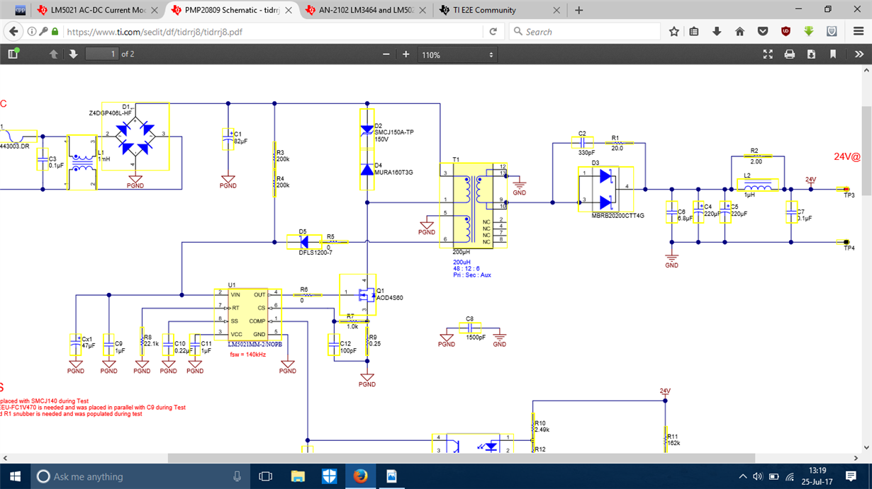
I am trying to use LM5021 to convert 220V AC into 5V DC.I have one doubt  from the reference design of LM5021.What is the purpose of D2 and D4? According to me only D4 should be there because when MOSFET (Q1)  turn OFF then D4 will provide a path for the current to flow through inductor (3-1) of transformer and prevent MOSFET from damage.But having D2 would prevent this current from flowing and due to this a large voltage can be appear on the Drain of the MOSFET and can damage it.

 e one doubt  from the reference design of LM5021.

  • Hello Sandeep,

    Both D4 and D2 are needed in this reference design, and countless other designs like it. D4 is definitely needed as you deduced, to provide a path for the leakage inductance current after the MOSFET turns off. D2 is also needed to establish a clamp voltage higher than the reflected output voltage. D2 is not a blocking diode like D4, it is a zener-type diode, but actually should be a Transient Voltage Suppressor (TVS) which is more rugged than a simple zener diode. If only D4 was present, then only about 1V of clamp voltage would appear across the primary winding and ALL of the energy stored in that winding during the Q1 on-time would be dissipated in D4 and none of it would transfer to the output. And D4 would burn out in a few seconds. To get the magnetizing energy out to the output, D3 must be forward biased, and that impresses Vout across the secondary winding, and that reflects to the primary winding by the turns ratio. So the voltage rating of D2 must be higher than that of the reflected voltage, or all of the magnetizing energy will be dissipated in D2.

    If the voltage rating of D2 is only a few volts higher than the reflected voltage, then it would take a long time for the leakage energy to dissipate and D2 would also dissipate much of the magnetizing energy. To limit the energy loss to only that in the leakage inductance, the voltage rating of D2 would have to be infinitely high. Obviously that is not practicable, so a compromise trade-off is made with the Vds max rating of the MOSFET to allow the clamp voltage to be reasonably high enough to absorb the leakage energy in a short time without losing substantial magnetizing energy at the same time. Typically, the clamp voltage is chosen to be approximately 2x the reflected voltage, so the total power loss in the clamp becomes 2x the leakage inductance energy x the switching frequency.

    Often, an R-C-D clamp circuit is used in place of the TVS at D2, because an RCD circuit can be less expensive. However, the RCD clamp voltage varies with the amount of energy put into it, so the clamping time is not constant and is more lossy at light loads. RCD clamps are often called snubbers, because they resemble an RC snubber, but their purpose at D2 is the same as D2: to be a voltage clamp for leakage energy to protect the MOSFET.

    Please see this Power Tip video training.ti.com/.../power-tips-snubbing-flyback-converter clamp design&tisearch=Search-EN-Everything for more information about the primary-side clamp.

    Regards,
    Ulrich