This thread has been locked.

If you have a related question, please click the "Ask a related question" button in the top right corner. The newly created question will be automatically linked to this question.

UCC27714: Please explain why no plots (datasheet) HO/LO output current relative temperature range

Guru 54057 points
Part Number: UCC27714
Other Parts Discussed in Thread: TIDA-00778

Hello,

Considering to change FAN73901 to UCC27714D but like to have some better idea of the HO/LO output drive current relative to temperature range. Datasheet makes huge effort to show numerous propagation delay plots versus temperature but not 1 graph plot of HO/LO output drive current.

Please elaborate what is HO/LO 250ma DC versus 4 amp peak and how that is achieved when HB/HS charge pump often has 1 amp fast Dboot diode, 1uf capacitor? Most 1 amp ultrafast diodes are tested for single 30amp 1/2 sine pulse but may have issues at 10Khz, who would know being 60hz is often used 1/2 sine testing. Would it not be better to use 2amp rated diode with a 100amp peak to achieve the HB/HS 4 amp peak after each pre-charge cycle without the cathode of Dboot clipping each current peak?

According to other engineers have explained the charge pump remains active in each PWM cycle in order for HO gate region to achieve Miller plateau in QGD in the HB/HS voltage offset far above COM.  Any thoughts how 10kHz to 100Khz PWM signal might effect the charge pump Dboot ability and gate driver HS/HB to maintain 4amps peak @-40*C to120*C?

  • Hello BP101,

    Thank you for your interest in the UCC27714 gate driver. I am an applications engineer with TI and will work to address your concerns.

    For the question about the datasheet graphs for the output current. The HO and LO rise and fall time with a capacitive load is a direct representation of the gate drive current capability, and that information is shown over temperature in Figures 10 thru 13. Since the gate drive output performance is dependent on the gate drive loop layout, it is more difficult to directly measure the current especially over temperature in a test fixture suitable for production. This is why you see the gate drive strength represented by the rise and fall times with a capacitive load.

    The HO and LO 250mA DC rating is related to typically a power dissipation limitation in the internal devices. Driving a capacitive load such as MOSFET's or IGBT's results in very low duty cycle peak charging and discharging currents with very low average currents.

    The charging current path for the HB-HS boot capacitor is sourcing the current from the VDD capacitor when the HS node is switched to COM by the low side power MOSFET. The gate driver current does not supply the HB capacitor charging current.

    On the boot diode charging currents, what you will generally see is on the very 1st charging cycle of HB there will be the highest boot diode current since the HB-HS boot capacitor is being charged from 0V. On the following switching cycles the HB-HS capacitor is not discharged very much with the energy required to drive the MOSFET Qg, if the boot diode is sized properly. As an example, if you have 10% ripple on HB which is on the high side, with 12V there would be only 1.2V drop. If there is a boot diode series resistor of 2 Ohms there would only be 1.2V/2Ohms or 0.6A current. 

    For the initial charging cycle, the boot diode needs some surge ability. Assume the boot resistance limits the current based on VDD - Vf of the boot diode. We recommend fast recovery diodes for the boot diode, also boot diodes with relatively low junction capacitance are recommended. These two recommendations are based on minimizing the amount of energy that may be discharged from the boot capacitor with high dV/dt reverse voltage on the boot diode.

    I hope this addresses your concerns.

    Regards,

    Richard Herring  

  • Hi Richard,

    Thanks for the quick response my friend. And I really like the ESD protection they put into the UCC27714!

    Richard Herring said:
    The HO and LO 250mA DC rating is related to typically a power dissipation limitation in the internal devices

    Seemingly indicates the sort circuit sink/source current yet where is any proof in datasheet 4 amps peak can be achieved other than it makes an unfounded statement backed up by no evidence of ever achieving 4 amps. The device perhaps had better dissipate well over 600mW sourcing @4A even by FAN73901 IC dissipation graph standards.

    Richard Herring said:
    The charging current path for the HB-HS boot capacitor is sourcing the current from the VDD capacitor when the HS node is switched to COM by the low side power MOSFET. The gate driver current does not supply the HB capacitor charging current.

    Actually LO does control the supply of VB current via Dboot to Cboot during pre-charge cycle and HS takes over when DBoot reverse biases each PWM cycle. In that regard Cboot charge depletes as you stated (1.2v/12v) but 12v VDD has never been used in any circuit TI has produced with NFET or IGBT modules or drivers that I know of.

    Richard Herring said:
    if the boot diode is sized properly. As an example, if you have 10% ripple on HB which is on the high side, with 12V there would be only 1.2V drop. If there is a boot diode series resistor of 2 Ohms there would only be 1.2V/2Ohms or 0.6A current

    I struggle with this idea being diode (If) limit should be calculated via Vf drop on Dboot at the peak expected current and not the supply limiting current. Similar to LED we figure the limit of current for the listed Vf drop of the LED, not the supply voltage. Given Vdd =15v and Dboot drop @1amp listed 0.9v, diode R is 0.9 ohms or R=E/I, actually much higher Vf drop @4 amps. We now have a 1 ohm 1/4 watt R in series with VDD into Dboot and 8.2 ohm 1/4 watt in series with VS pin, similar to HS pin for when the diode enters reverse bias as HO turns on GS saturates and DS current flows into HS pin and Cboot receives a small V drop.

    Another FE suggested VDD charge pump automates after pre-charge boot strap cycle, yet the story seems incomplete. The repeating dip we see in VDD is due to charging Cboot each PWM cycle and you say only by a small amount. Yet is not Cboot (entirely discharged) by LO HI side switching ON in half bridge PWM cycles 3 phase inverters? Indeed one thinks it should be entirely depleted, so Dboot then has to source (full) VDD current each and every PWM cycle. 

    Perhaps the panic if UVLO drops below 4v/12v has roots in Cboot charge path and reverse current path via LO on cycles and the need to turn off LO rapidly as possible? Note worthy is voltage clipping at a diodes cathode can result when or if current exceeds peak (If) current of the device. Reason and idea to suggest a 2 amp Dboot with 4 amp gate driver as the NFET GS seemingly requires to be rapidly saturated via Cboot in the faster slew rate of QG and Dboot must then handle the peak VDD inrush (If) current into Cboot as LO switches on. Tina might help in that analysis to prove just how much inrush peak exists.

    That is if the UCC27714 can sustain 4 amps for long and again no pulse test curves relative to duty cycle or temperature rise exist to verify it actually can. I will look at plots again and try to understand how 4 amps can be reached by LO/HO outputs. Also no HS pin plots of allowable negative voltage over the 40-120*c temperature range exist.

     Speaking of HS and Cboot, does not the current path change from VDD/VSS on Cboot discharge and swing to VB/HS during Dboot reverse bias, thereby depleting Dboot via QG? And should we then calculate the peak diode current relative to the expected Vf drop at the required peak current via HB/HS of NFET for our total QG or gate charge?  I think you mention MOSFET QG but why is there no R value in series with HS pin and should we also consider or calculate Dboot (If) relative to MOSFET QG?

    The test results of figure 53 failure mode and text seem to leave out what or how to prevent the negative dv/dt at the HS pin and why is HS so prone to negative spikes if noise canceling circuitry reduces dv/dt at the HS pin, by how much negative voltage does it cancel dv/dt? Judging by figure 53 canceling circuitry seems to allow -80 to -18v to ride straight into HS pin and effect the HO output level.

    So any voltage down to or above -18v is ignored by HS input and that is a fantastic test result by any standard a new bench mark?

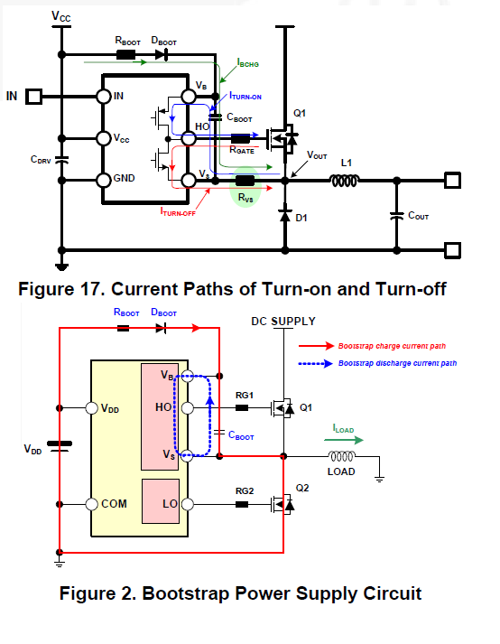
  • Example to help clarify how HB cap (Cboot) does indeed discharge via HO current path each PWM cycle. So it seem the actual HB cap charge via (Dboot) or HB diode could be significant.

    Note no current trace capture (Dboot) is ever presented in TI analysis captures, leaves one to suspect more current than expected may traverse though HB diode in each cycle.

    Illustrations other vendors (great) research effort to clarify the boot charge cycle current paths:

  • Hi Richard,

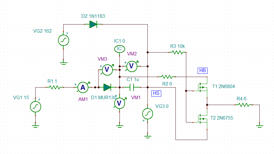
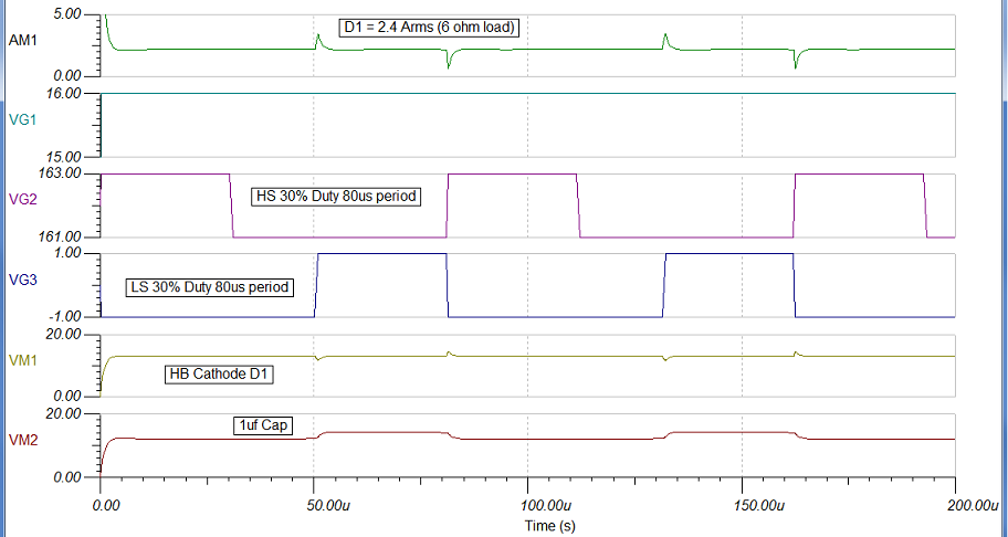
    I did a Tina analysis on HB boot diode current using an internal gate driver totem pole for the Pre bias model and see 2 amp sustained 3.5 amp peaks with 6 ohm gate load @12.5Khz. The1000pf input gate load (Figure 10-13) seems very little compared to 4600pf (Ciss) total (109Qg) for the parallel NFET's we expect to drive with UCC27714.

    Still fail to understand how datasheet figure 10-13 proves HO/LO outputs can sink/source even 1 amp let alone 4 amps. TIDA-00778 figure 33-36 show UCC27714 HO sink/source 2amps and 0.55v ripple exists across Cboot @15kHz PWM. Point is why not do the same load test for UCC27714 datasheet using fan cooled inductive load jig and MOSFETS with actual (Qg) load.

    Simulating Tina gate drive current @HO indirect 6 ohms gate drive equals HB diode inrush current during each charge cycle of Cboot may suggest higher slew rate of UCC27714 LO/HO actually sources more VDD current via HB diode than simply 1 amp. It seems the best way to know for sure is not to guess but to simulate what could be the actual function.

    Perhaps a spice model of UCC27714 might give me better understanding - does one even exist?

  •  Hello BP101,

    The peak current in the boot diode is dependent on the resistance in series with the boot diode. If there is no resistance in series with  the boot diode , then the peak currents are limited by boot diode  internal resistance, low side FET on resistance and layout parasitic inductance. We recommend an external resistance in series with the boot diode to limit the initial charging peak current when the HB capacitor is charged from 0V. This also makes the repetitive peak currents less dependent on semiconductor internal resistance.

    The 2A to 3.5A peak currents with a simulation that does not include parasitic elements such as trace inductance, is not unexpected. Are the 2.5 to 3A peaks a concern? A 1A DC rated diode can typically sustain much higher peak current

    For the statement of the application equivalent capacitance of 4.6nF Vs the datasheet graphs at 1nF. We are aware the application will many times be with a higher equivalent capacitive load. If you look at many of the drivers in this category, you see the test data typically at 1nF or maybe 1.8nF. The rise and fall time parameters at the same capacitive load makes comparison of the rise and fall time performance consistent and easier. You will likely never see a driver specified at the specific conditions that you have in any given design.

    The UCC27714 could not be released advertised as a 4A driver unless the parameter is achievable as the stated typical value. The TIDA design referenced has external gate resistance which will affect the gate driver current. I recall it is 4 Ohms turn off and 6 ohms turn on.

    There is a PSpice model available for the UCC27714 at the following link: www.ti.com/.../toolssoftware

    Regards,

    Richard

  • Hi Richard,

    Richard Herring said:
    A 1A DC rated diode can typically sustain much higher peak current

    We would hope as most datasheet boast 30 amp surge for one half cycle (only) at 60Hz not 10.5Khz for a 1 amp ultra fast diode (Trr<=14ns). Yet Tina transient indicates as HS pin swings negative by even 1v below & above VSS with HB following in 1-2 volts the boot diode current becomes more periodically above even 2 amps with a 2.2 ohm series resistor. Notice the TIDI-00778 figure 36 ripple across Cboot varies VDD by 0.5v, that ripple actually represents over 2 volts drop in VDD relative to HS dropping below VSS/COM.  As HS swings even more negative below VSS (VG3) the current through Boot diode grows exponentially above 1 amp during the time HS remains in a prolonged negative state. Have to assume the MOSFET load and VDD drop has much to do with the total current through HB boot diode and how long it sustains that current dependent on the inverters DC load.

    Richard Herring said:
    The rise and fall time parameters at the same capacitive load makes comparison of the rise and fall time performance consistent and easier

    Sorry it makes little sense to me when other vendors datasheet list exact HO/LO sink/source current in a periodic range (<10us). The UCC27714 does make the claim (Iout) pulsed (100ns) +/-4 amps in the AMR section. Obviously (Iout) can reach 2amps (@15kHz or 66.6us) TIDI-00778 figures 33,34 proves 2 amps sustained 15kHz and beyond 2amps must be <100ns? So pulsed 100ns only at very peak of 4 amps but what about 2 or 3amps, ok at any pulse period?

    Thanks for the Spice model link : )

  • Hello BP101,

    In the case of HS negative voltage which does occur in many power trains, the HB capacitor can be charged to Vdd-Vf of the boot diode plus the negative spike. In this case it is even more important to have resistance in series with the boot diode to prevent voltage spikes from peak charging the HB-HS boot capacitor.
    On each cycle the boot capacitor negative ripple will be due to the energy to charge the MOSFET gate charge and the HB quiescent current. If the HB capacitor is charged to a higher voltage from the HS negative spike, and the HS negative spikes are relatively consistent, the boot diode charging current will still be based on charging the boot capacitor based on the gate charge and quiescent operating current.
    The UCC27714 datasheet does not have the peak current Vs time operating curve. Based on the effective gate capacitance of 4.6nF mentioned you should not have a concern about the peak current duration.

    Regards,
    Richard Herring
  • Richard Herring said:
    the HB capacitor can be charged to Vdd-Vf of the boot diode plus the negative spike

    Good points you make:

    Tina analysis if we cycle HS (12.5kHz) from 0v to 1-v below VSS, a spike occurs in (If) through boot diode in both directions. Makes sense as the VDD potential suddenly returns from being pulled down a current spike occurs through the diode. Even with 2 amp diode @0.9v drop, 2.2 ohm series R the current average remains above 2 amps. Again that occurs relative to pulling HS by only 1-v below VSS at 12.5khz

    You would think any HS negative spike from switch node (dv/dt) would vector into the ground side of HB capacitor thus lower or subtract from VDD potential as occurs in transient analysis. Thus diode current would dip during the charge cycle of boot capacitor pulling VDD charge across Cboot down not up. Relative to a 3 phase inverter that is and (dv/dt) can travel along ground from other fired phases while the boot cap is being charged in another 1/2 bridge. In any case we rated Cboot @100v just incase the drop is severe during (Trr) of boot diode.

    Richard Herring said:
    Based on the effective gate capacitance of 4.6nF mentioned you should not have a concern about the peak current duration.

    Confusing me further is Output Block section shows +/- IGKPT short circuit pulsed current (PW <10us = 4A) seems to contradict AMR 6.1 Iout pulsed (100ns) +/-4A .

    What's the difference here or is 100ns a typo?    

  • BP101 said:
    Tina analysis if we cycle HS (12.5kHz) from 0v to 1-v below VSS, a spike occurs in (If) through boot diode in both directions.

    Referring to the Tina model posted above with LI=100-ns pulses (VG3) to simulate (dv/dt) spikes on HS pin traversing below VSS or COM.

    For some odd reason the down loaded Spice model of UCC27714 allow high voltage to pass out the HO pin when HS input is tied to the inverter bridge NFETS. If HS pin is not connected the HO output signal is void.