This thread has been locked.

If you have a related question, please click the "Ask a related question" button in the top right corner. The newly created question will be automatically linked to this question.

PMP3162: Help for PMP3162 debugging. DC/DC 36~72V in, 12V/16A Active Clamp Forward.

Part Number: PMP3162
Other Parts Discussed in Thread: UCC2897A, PMP20742, UCC27511

Hi Guys,

I do not have too much background of DC/DC converter design.

I just found the PMP3162 could meet our reqirement through google searching.

All the circuits parameters are same as reference design of PMP3162.

Excpt 2 parameters chage as below (out DC/DC output has change to be 12V and around 5A):

1, T1 (PA4141NL)  has changed to be PA0273NL, as below:

2, L1 has changed from PG1083.682NL to PG0871.682NL (Similar Inductor value just different in Irat);

 We found there has no output (Voltage of Vout kept 0) after we powered on the modified circuits, looks like the UCC2897A does not active yet.

So, anybody can offer me simple guide about how to debugging this circuits?

Looks like I can start to adjust the Resistor on Ron, Roff, RTDEL, RSLOPE, LINEUV, and LINEOV, or the resistor connected with opto-coupler, right?

Thank you for your reply!

  • Hi Bo Zhang,

    Thank you for your interest in PMP3162. I would start by confirming the input voltage is getting applied to the UCC2897A controller. Check if you see a reference voltage. Then check if the gate drive signals are getting generated. Then check if the bias voltage is getting generated and check the output of the gate driver.

    Best Regards,
    Ben Lough
  • Hi Ben, Thank you for your feedback,

    Our "PMP3162" been powered with 48V DC, checking items as below:

    1, VIN of UCC2897A, 48V DC is normal;

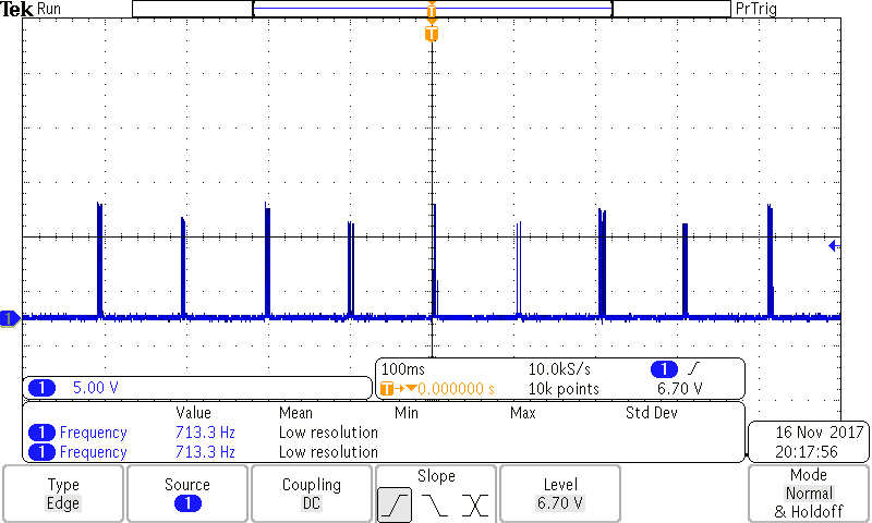
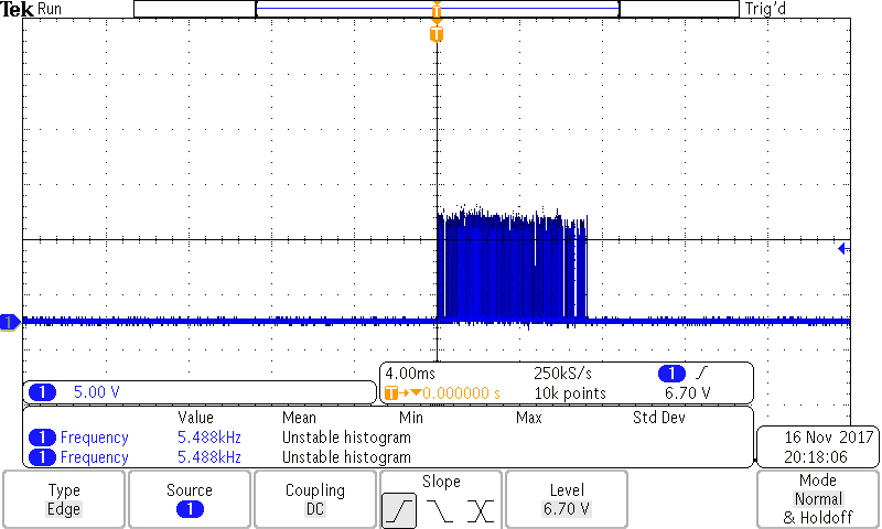
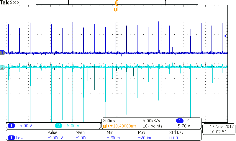
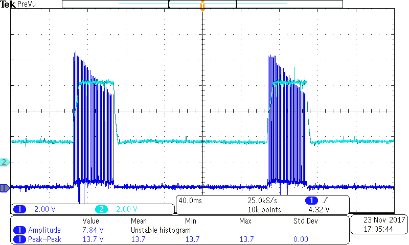
    2, Driver signal for G of Q4 and Q6, an un-continued drive waveform could be captured as below:

    A reverse signal could be captured at drive signal for clamp route (G of Q3, P channel mosfet);

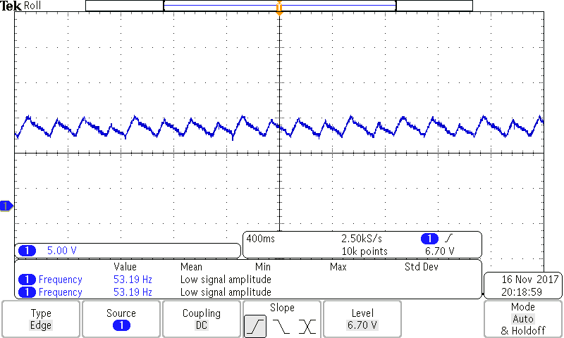
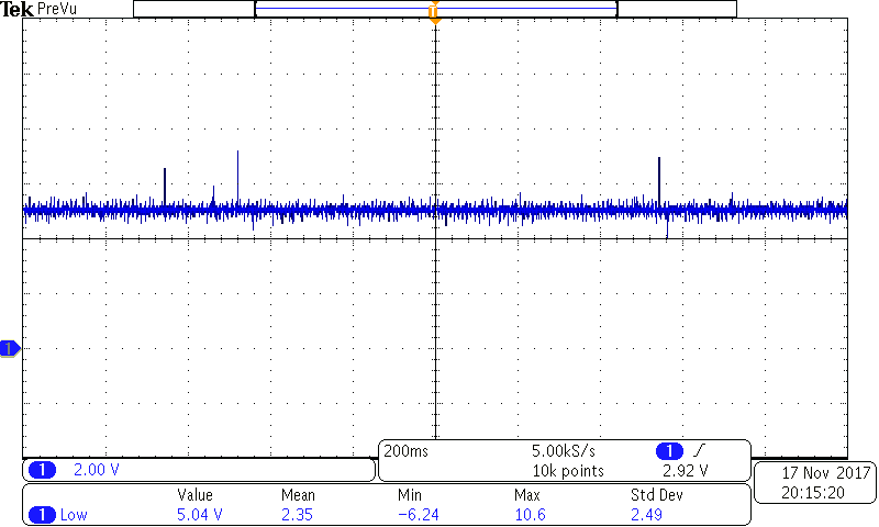
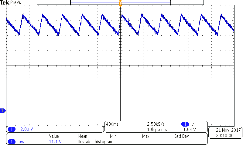
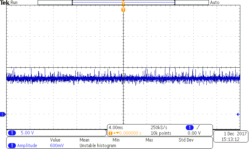
    3, Waveform of Bias signal as below:

    4, Only about 3V (not 12V) voltage could be measured by MM at output (empty load).

    Looks like some protection function been switched on and off sequently, right?

    So, what is the next step to debug it?

    Thanks

    Bobby

  • Hi Bobby,

    The bias voltage looks low. It should be above 8V. Can you check the voltage of the REF pin? Also check the waveform of the CS pin. You might be tripping hiccup mode protection. 

    PA0273NL and PG0871.682NL may not be suitable replacements for the original transformer and inductor. PA0273NL has a current rating of only 4.5A on the secondary and PG0871.682NL has a current rating of 5.8A. These will likely saturate trying to supply a load of 16A. Have you tried contacting Pulse electronics? They could supply the original custom magnetics used in this design.

    Best Regards,

    Ben Lough

  • Hi Ben,

    Our project shrinked the output capability of this DC/DC converter, from 12V/16A to 12V/5A. (May change to 12V/16A in future).

    That's why we changed the parameters of T1 and L1.

    After one day's debug, Here is the update:

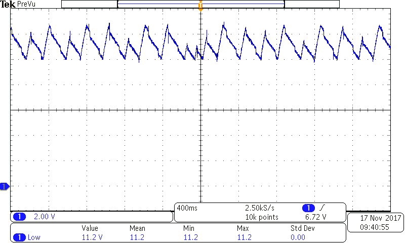
    1, Bias voltage should OK, minimum value is around 11V, waveform as below:

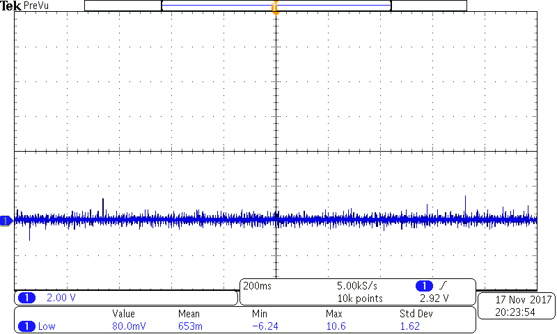
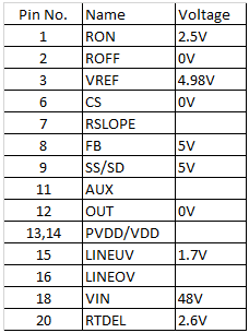
    2,  REF voltage (pin_3) is normal (5V),  as waveform below:

    3, Voltage on SS as below:

    But voltage on CS almost remained to be 0, waveform as below:

    Compare the waveform on G of main MOSFET with pin_1 of current sense transformer T2, waveform as below:

    CH1: Drive voltage on G of Main MOSFET Q4 and Q6;

    CH2: Voltage waveform on pin_1 of T2 (current sense transformer);

    This is the waveform confused me the most, why all the pulse on pin_1 of T2 are negative, so, the D4 will never be conducted.

    Based on my limited basic idea for transformer, the pulse here should be positive, right?

    So, could you offer me guidance for what is the next step to debug it?

    Thanks

    Bobby

  • Hi Bobby,

    Thanks for the waveforms. I agree, the current sense waveform does not look right. Could you check the voltage waveform across the current sense resistor R3?

    Best Regards,
    Ben Lough
  • Hi Ben,

    We found the Pin_7 and 8 of T2  have been switched in layout package, after we switch them back, Output voltage still kept 0V.

    Test result as below:

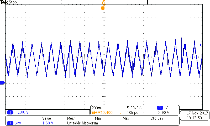
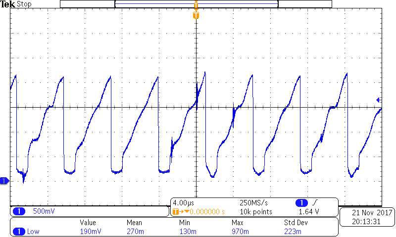
    Waveform of BIAS as below (And a synchronized waveform could be observed on AUX):

    Waveform on RSLOPE as below:

    So, what is the next step?

    Thanks!

    Bobby

  • Thanks for the waveforms Bobby,

    Could you check the waveform of the CS pin after switching the pins on T2? I would then check the voltage on the SS pin to make sure it is not clamping the duty cycle. Could you also take another waveform of the gate drives (OUT and AUX)?

    Best Regards,

    Ben Lough

  • Hi Ben,
    I did not offer the waveform on CS, SS, and Out, cause they appeared to be a constant DC value on the scope.
    Almost 0V on CS pin;
    And 5V on SS pin;

    Strange to capture a similar waveform for AUX and BIAS,
    For OUT pin, alos a constant dc value around 0V;

    1, Looks like the UCC2897A not start working, will check more details tomorrow;
    2, Will try to replace the T1 transform to check if something wrong with it;
    3, Will check their waveforms during power on stage tomorrow;

    let me know if you have any suggestion.
    Thanks
    Bobby
  • Hi, anybody still there?

    Update as below:

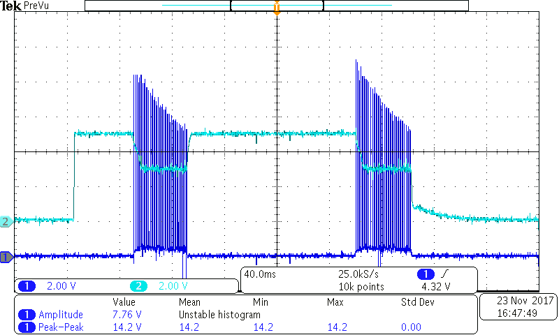
    Controller start work, almost empty load, but PWM waveforms kept on/off perodic, compare the waveform on G of Q4, Pin_4 of opto-coupler, as below:

    Channel_1: G of Q4 and Q6;

    Chaneel_2: Pin_4 of U6;

    And compare the waveform on G of Q4 and Voltage waveform on Vout port (J2), waveform as below:

    Channel_1:G of Q4 and Q6;

    Channel_2: Output voltage output;

    Question:

    1, looks like the Vout at J2 make the opto-coupler satured, does that mean we can inrease the value of R20 to keep the PWM waveform away from shut down?

    2, The output voltage could not reach to 12V, only about 6V, what we can do to make it boot to 12V?

    Thanks

    Bobby

  • Hi Buddy,

    I am still alive.

    I change R5 to 1.27ohm and R20 to 5.1Kohm,

    Now, the Vout boot to around 12V, but the transformer is very hot under light load (around 500mA) in short time.

    Now the question change to be: What I need to change to make the parameters of the circuits (PMP3162) to accommodate the shrinked transformer and output inductor parameters:

    1, Duty cycle (May not); 2, Current sense loop; 3, opto-coupler loop;

    Thanks

    Bobby

  • Hi Bobby,

    You want to make sure the new transformer and inductor do not saturate at full load. You will want to take a look at the primary side transformer current as well as the inductor current on the secondary. Have you been able to run the converter at full load?

    Increasing R20 will reduce the fast lane current through the opto. I would suggest taking a bode plot of the converter to make sure the bandwidth and phase margin is still acceptable.

    Best Regards,
    Ben Lough
  • Hi Bobby,

    I would like to suggest an alternate transformer for your design. Please take a look at PA2398NL. The lower magnetizing inductance should help with the heating problem you were seeing. This transformer has been used in other active clamp forward designs in the power range you are interested in such as PMP20742.

    I also suggest increasing your inductance to ~10uH. You can get away with less ripple current at 5A vs 16A and it will make compensation a bit easier. The final compensation values will look very similar to the feedback network of PMP20742 if you have a similar output capacitance.

    Other suggestions:
    Since your power level is 60W, you can eliminate a few other components in this design to save size and cost.
    1. The primary and secondary currents are much lower for an output current of 5A than 16A. 1 primary side NMOS should be sufficient so you can get rid of Q6.
    2. The snychronous rectifiers will not need parallel mosfets as well so you can also eliminate Q2 and Q7.
    3. You can get rid of the current sense transformer and just use a current sense resistor connected from the primary side NMOS source to ground. This will be a little less efficient than using a current sense transformer but it's much cheaper.

    I hope this helps and please let me know if you have any additional questions.

    Best Regards,
    Ben Lough
  • Hi Ben,

    Thank you for your suggestion.

    I will keep optimizing the current project and update here the progress.

    Thanks

    Bobby

  • Hi Ben,

    Now the situation is: increased the resistor value of R20 to make the output voltage booted to 12V.

    For available parameters configuration, we found the MOSFET (Q1, Q2, Q5, Q7) connected with the secondary side of transformer (T1) will turned to be more hoter (Than transformer).

    In fact we did not connected a heavy load to the output of the DC/DC, The current output is only around 1A.

    As I know, the Q1 Q2 and Q5 Q7 will turned to be on/off sequently, according to different power stage.

    Is it caused by there has no enough drive capability of UCC27511, so, all the current on secondary side of T1 was burndened by the body diode of MOSFET?

    Or these MOSFET''s on/off time is mis-aligned with power stage of the primary transformer side?

    Will check more detail tomorrow and any suggestion are welcome.

    Thanks

    Bobby

  • Hi Bo,

    I would check the VDRV signal to make sure the gate drivers are getting power. The switching of the rectification mosfets are determined by sensing the voltage on the transformer windings. I would compare the waveforms of SEC1, SEC and the output of each UCC27511 to check for misalignment. If that looks ok, take a look at the VDS waveforms of Q4, Q1 and Q5 and compare it to section 8 of the test report for PMP3162.

    Best Regards,
    Ben Lough
  • Hi Ben,

    Here is my check result.

    Waveform below was captured at E pin of Q8, it was a constant voltage value around 12V:

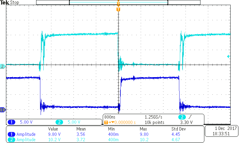
    Waveform below was captured at OUTH, OUTL at UCC27511 (U1 and u4);

    Ch1 was captured at OUTH & L on U1;

    Ch2 was captured on OUTH & L on U4;

    Looks like the drive capability of UCC27511 in thus configuration was enough;

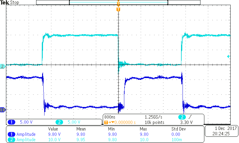
    Compared waveform also captured on OUTH & L on U3  and U1, waveform as below:

    Ch1: OUTH & L of U1;

    Ch2: OUTH & L of U3;

    Looks like the lag between the OFF of Q2, Q1 with the ON of the main loop Q6 and Q4 was around 200ns;

    This should not be a serious mis-alignment? right?

    So, question now is:

    If this lag was not a serious mis-alignment, why the MOSFET (Q1, Q2, Q5 and Q7) was so hot?

    Thanks

    Bobby

  • Hi Bobby,

    It is normal to have some dead time between Q4/Q6 and Q2/Q1. This is primarily to prevent shoot through. How hot are the FETS becoming? Are you able to take a thermal image?

    Best Regards,
    Ben Lough