This thread has been locked.

If you have a related question, please click the "Ask a related question" button in the top right corner. The newly created question will be automatically linked to this question.

UCC28630: Odd Vsense and fault latch on UCC28630

Part Number: UCC28630

I have powered up a new flyback design using the UCC28630 (Custom design/layout).  All models and most of the layout has been verified.  

I have been scratching my head over the current issue, since it seems like the circuit should be working; however, when powered on from 120VAC, the VDD pin bounces between 8V-10V as if there is a fault latched on the chip.  There is never a DRV PWM voltage and the Vsense pin reads 5.5V at the time of the latched fault.  When observing the SD pin, I am seeing a 30us pulse, followed by 21x 1us pulses.  This tells me according to other people's post that I have an open or short on Vsense. 

I turned the circuit off and removed and tested the resistors and everything tests well as though the fb circuit should be operating normally. 

What else could be causing this?

As a side note, the pulse train at VDD never reaches a proper peak voltage.  They appear more as low amplitude pulses (0.5V).  This circuit also, only has a 10k load populated on the secondary side of the flyback transformer right now.  Would this generate issues?

The feedback resistors are 27k, 35.7k with a 0.16 primary to auxiliary turns ratio.  I can send a chunk of the schematic if necessary, though I am really just looking for places to hunt.

  • Nicholas,

    Can you post your schematic with values?

    In particular, the resistors on the VSENSE pin must have a Thevenin equivalent value in the range of 10-20 k-ohm – outside that range, it will be detected as a possible open or short on the VSENSE pin, startup will be aborted, and the fault code #21 will be reported, as you are seeing.

    However, if you are using 27 k & 35.7k, the Thevenin is 15.37 k, right in the middle of the range. Do you have anything else connected to the VESNSE pin or the aux winding?

    The output preload will make no difference for this issue.

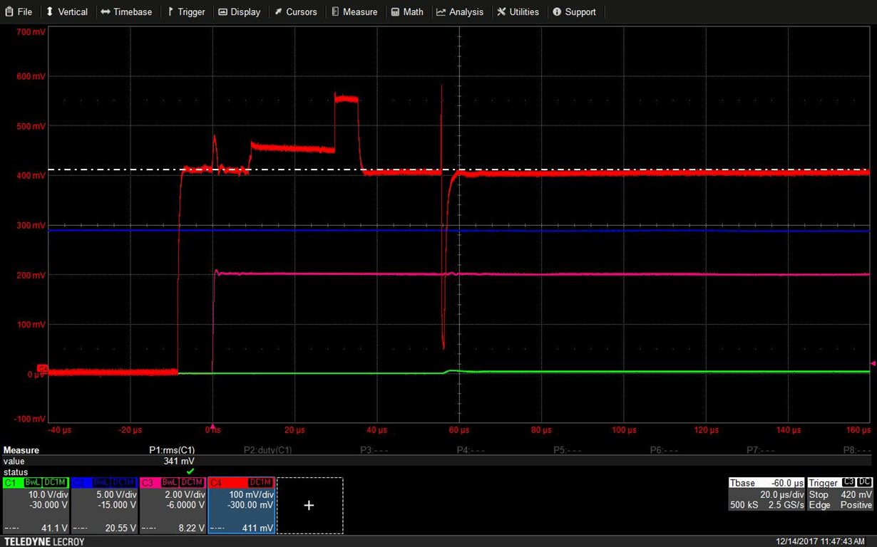
    Can you put a scope probe on the VSENSE pin and capture the waveform when the IC first starts up? You could trigger on the rising edge on the SD pin, this will transition from 0 to ~4.5 V shortly after the VDD reaches the start threshold of ~15 V. You should look at the VSENSE pin at ~ 100 mV/div, and with time scale ~10-20 us/div.

    This waveform was taken on UCC28630 EVM572, and the initial level of ~411 mV is the level set as a result of the VSENSE Thevenin resistance of ~13.25 k-ohm.

    For your Thevenin of ~15.37 k, this level would be expected to be ~460 mV. If this level is < ~300 mV or > ~600 mV, this will trigger a VSENSE fault.

    If this is happening, and the resistor values are correct, something else must be pulling up or pulling down on the pin. Or maybe you have excessive capacitance loading the pin?

    Thanks,

    Bernard

  • Bernard,

    I've combed through the datahseet/equations and most everything checks out.  The layout as well.  Right now, this is what I am seeing.

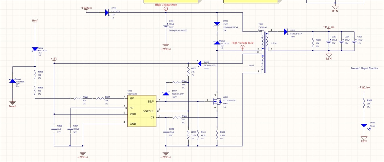
    First, here is the schematic snippet of that supply, though there is much more going on since this is a motor controller design.

    I have been probing the SD pin along with the Vsense pin and this is what I see.  There is a slow rise of Vsense, then SD starts to come up, and both lines cut off down to ground.

    Is it possible that the extra capacitance on SD is convincing the Vseene check that there is too much capacitance on the line?

    The rise time of Vsense is very, very long.  I am not sure why.

    For reference Vsense is channel 1, SD is channel 2.  I am unsure as to why Vsense would appear loaded unless I have put too much capacitance on VDD/SD.  If I do not hear back too soon, I will begin playing with those values.

    Slight edit/update.  I removed C307 per the datasheet description and I have a slightly clearer picture.  See below.

    What is odd to me is that prior to the sample, my sense line is high when your sense line is low.  I see no changes/action on the DRV pin either which would be the source of any kind of pull-up through the 3.9k.

    I can see how this would generate a fault since the line is sampled at 760mV, though I do not know why in the current configuration.

    Thank you,

    Nick

  • Nick,

    I can see the error - you have connected the top of the resistor divider on VSENSE to the DC side of the aux diode D305, so it's actually connected to VDD.

    The top of R302 should actually be connected to the anode of D305. This change should fix your problem.


    Thanks,
    Bernard
  • That got rid of the Vsense fault. Thank you Bernard, there is a reason that TI/Unitrode has been at the center of my power supplies. You guys have all of the answers!

    The current circuit is unloaded and throwing a VDD fault due to a ring on VDD. I am going to add a dummy load and some downstream circuitry to see if that solves that issue.

    This does bring up one other interesting question now that I am here. What is the best way to compensate a flyback that works in this mode? Normally I would use the standard isolator reference filter on the isolated side, but this circuit is very different than the flybacks that I am accustomed.
  • Nicholas

    I would recommend adding a small R is series with aux diode D305, this will help prevent VDD pumping up due to leakage inductance energy. But that is usually only a problem at heavy load. The resistor value is typically a few ohms, 4R7 to maybe 22R depending how much leakage inductance you have in your transformer.

    If you are hitting OV on either VDD or the main output, then you may not have enough pre-load power in R301. The datasheet and design calculator will recommend the right value for R301 – once the controller drops to Fmin, a certain min power will be transferred (0.5 * Lmag * Ipkmin^2 * fswmin), and the preload needs to absorb this power level (aim for maybe 2x to give margin to Fmin for regulation).

    I think that R310 needs to be more like 2k2 based on your sch values, but eqns. 64/65 in the datasheet covers this.


    As for the loop compensation, this is internal to the PSR controller, you don't need to worry about it.


    Thanks,
    Bernard
  • Bernard,

    I recalculated pre-load power around 21mW which gives a ~4k value for R301 at 15V.  I doubled down on your double down (1k, R301) while testing and I am still seeing parasitic rings.

    I have thrown in a 3.9 ohm resistor as a source impedance to the auxiliary diode (D305) and the ring persists!  I suspect that I have created this issue by trying to go cheap on this experiment.  The lesson I am relearning is that motor controllers/SMPSs need a ground plane beneath the top layer.  Anyhow.. I am adding a few 14 AWG wires between the VDD cap, the GND pin, and the bottom of the current sense resistor to minimize ground parasistics as well as adding a gate drive resistor to slow up the FET to see if this helps.  If I am able to get this working, I can work out firmware while I wait for a new board spin.

    This project was originally rushed, but since I now know that I am going to miss the deadline I am considering a re-spin.  Before I re-spin with the UCC28630, I wanted to ask you a question.  I have a 5V linear regulator and a few opto-isolators on the VDD side of power.  I noticed that when I loaded VDD with around a 1k load, VDD would not start up.  I am all for using this chip since it actually has some pretty advanced features and I am blaming these issues on my rush, however, if this chip is unable to source power on the VDD/auxiliary side of the flyback, I will probably need to move back to a more traditional flyback design.

    Would you recommend this chip for a combination auxiliary and output side circuit or output side only circuit?

    Thank you in advance.

    Nick

  • Nicholas,

    If you want to power up other loads from the primary-referenced 15-V VDD rail, then you will need to decouple them from the IC VDD rail to allow the IC to start up.

    I assume that you do not need to be able to supply power to these loads while the VDD rail is charging up through the HV pin?

    The HV pin can supply only a limited amount of current out through the VDD pin to charge the external VDD cap C306. You should avoid connecting any loads directly to C306/VDD pin.

    You need to use another rectifier diode same as D305 and another cap, and connect those to the aux winding to generate the 15-V rail to power the other loads.

    This allows the HV current source to charge the VDD cap C306 while the other 15-V loads are decoupled, and VDD will always charge to the start level regardless of these other loads. When the IC starts up, the 15-V primary rail will just be another output on the transformer just like the main output 15V_iso that will also have to have its output cap charged and its load supplied - just like a multi-output Flyback.

    The power drawn by the primary 15-V rail should be added to the main rail to ensure that the total power is accounted for in the power stage design.


    Let me know if this is not clear and I will try to find a schematic to illustrate.

    Thanks,
    Bernard
  • That is perfectly clear. I will split out power to a second diode. This board is cut up enough that it shouldn't make a difference at this stage.

    Any idea on the ring or proceed as planned? I will be science fairing the next two days with my hardware hat, so if you see anything I missed, it would be appreciated.

    Nick
  • Nicholas,

    I re-read your previous post and here are a few more comments:

    - I did not realise that there was no gate resistor - this is highly recommended, esp since the driver is quite strong - there will be very large peak currents flowing every time the FET turns on and turns off, causing a lot of ringing.

    - I would recommend a few 10's of ohms for the gate resistance. Or use a large-ish turn-on resistor with an anti-parallel diode and smaller value resistor for turn-off, similar to the EVM. I think this could resolve a lot of your issues.

    - For the scope plot of VDD, where/how is this measured, is there a big loop area for the scope probe GND clip?

    - Did you use the Excel design calculator on the TI product folder to generate the power stage?
    (www.ti.com/.../sluc537)

    - The Rcs value seems very low in combination with the high value of inductance. Ipkmax ~0.8/0.3 = 2.67 A seems quite high for the 1-A rated MOSFET being used.


    Thanks,
    Bernard
  • Bernard,

    Thank you.

    I am actually quite experienced with Flyback/buck/full-bridge design and I keep my ground loops when measuring around 0.5" with the ground lead wrapped around my probe. That is definitely not artificial coupling by rf.

    We were rushed by a customer and ended up making a WEBENCH special, but now I am back at the drawing board doing a more thorough design. I had selected a low Rcs with a plan on stepping it up once I had a better idea of what the chip was capable of. This will likely be closer to 0.5/0.6 by the final rev.

    I have been going through the calculator since yesterday and I am updating and improving a few values. I will post a final schematic when I have all of the odd quirks pushed out so that someone implementing this may have a walk through on some of the more subtle problems associated with an off the cuff design.

    Nick
  • Bernard,

    On the first day I walked up a gate resistor and anti-parallel diode to 300 ohms and 10 ohms.

    Here is the ring at 100 ohms and 10 ohms:

    Here it is at 300:

    I am noticing my regulation voltage move around a bit so I adjusted the Vsense network to 27k Ra and 24.9k Rb, but I am still seeing an overvolt condition, so I ended up moving moving a parallel diode and loading 1k on the auxiliary power supply and 330 ohm on the +5V outputs on either end of the PSU.  I may have overloaded, because my final output is not an auto-restarting VDD undervolt condition.

    VDD:

    Output:

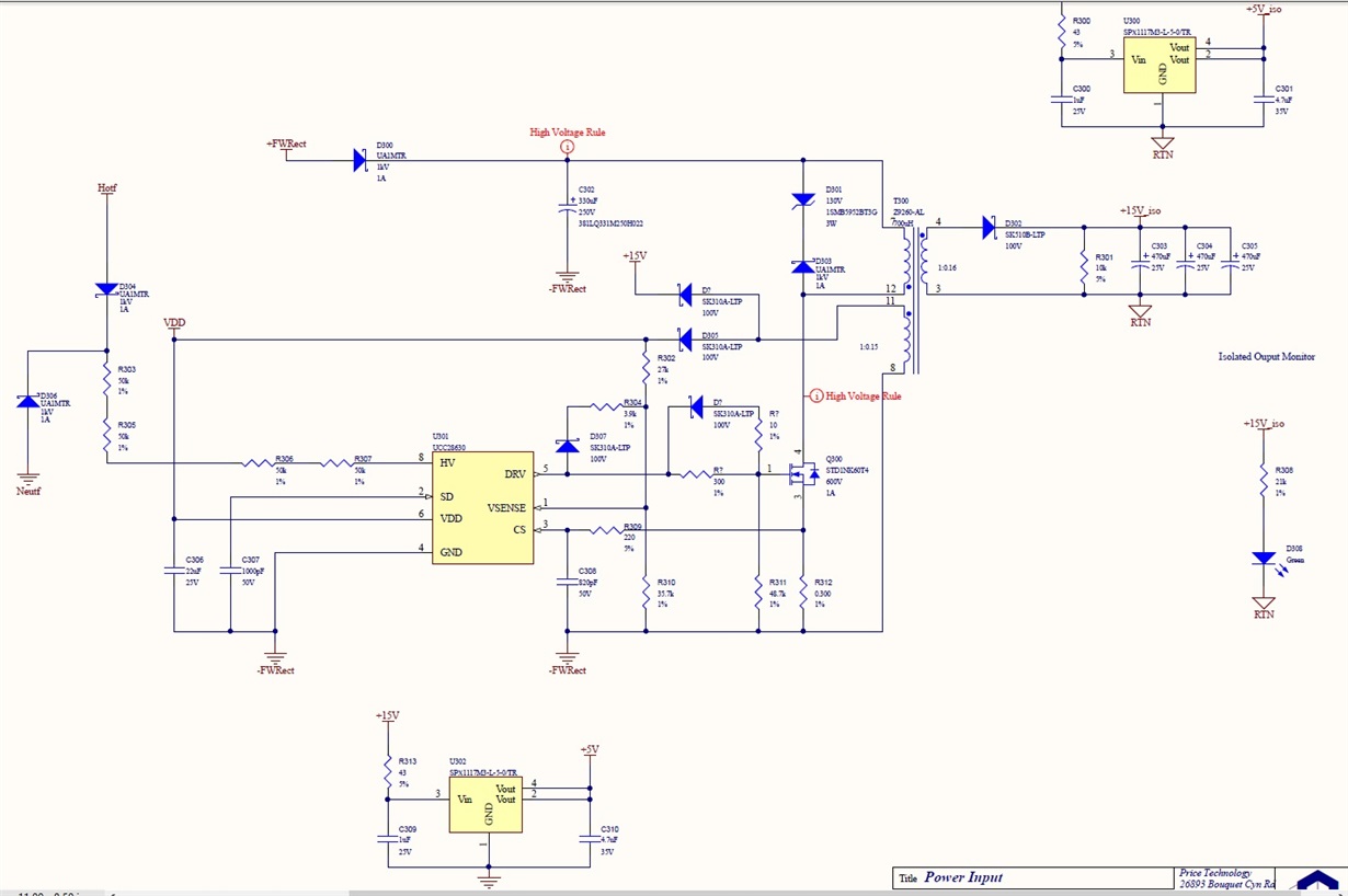
    Here is what the current schematic look like minus my DC loads:

    From here I am going to walk back my aux load to about 2k and start tweaking current sense with the feedback network, but this seems like I am threading quite the needle.  Any feedback you have here would be appreciated!

    Nick

  • Bernard,

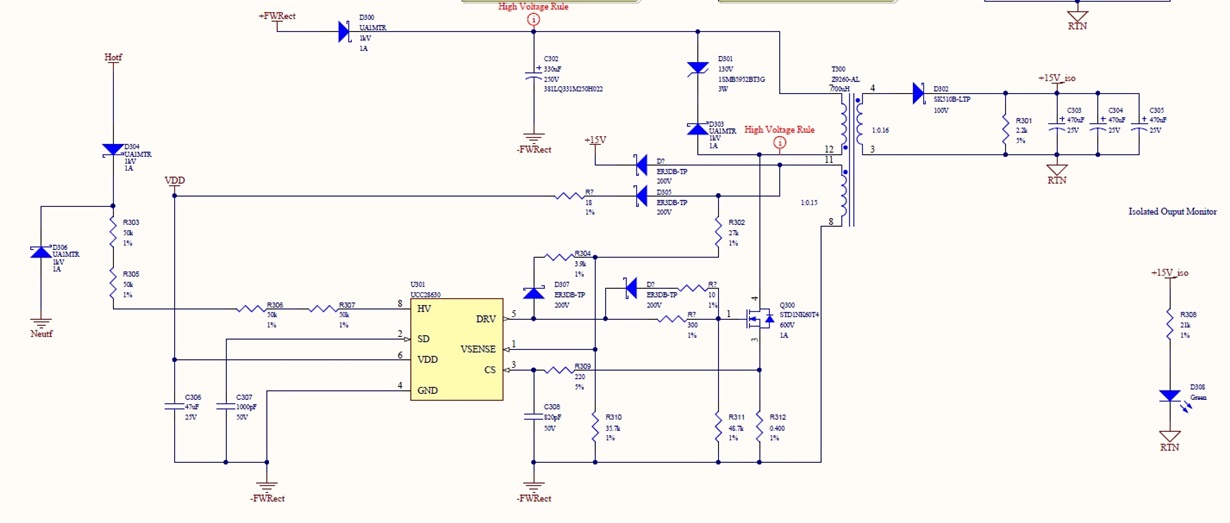
    All is good now.  I appreciate your help.  The final schematic is below.

    There were two additional issues.  The VDD cap was not large enough to hold up during soft start and that was causing an undervoltage trip.  Once that was straightened out, there was a constand overvoltage trip after softstart.  That was caused by the Rp diode (D307).  The reverse recovery was greater than 100ns, so large errors were causing bad regulation.  Once that was straightened out, the entire circuit stabilized and I was able to tune the output to around 15.5V, no problem.

    Thank you.