This thread has been locked.

If you have a related question, please click the "Ask a related question" button in the top right corner. The newly created question will be automatically linked to this question.

UCC27211: HO and LO missing pulses at low temperature

Part Number: UCC27211

Hello,


I have some problem with the functionality of UCC27211 gate driver at low temperature (from 10degC downwards).

I wonder if someone from technical support will be able to help me.


The application is a non-isolated buck converter. The UCC27211 is used to drive the conduction mosfet and the synchronous rectifiers.


The driver operates fine at ambient temperature, but when it is tested at 10degC oven temperature or below, the HO and LO stops once every few pulses.

I am able to replicate the problem with several different test units, and I am able to replicate the problem by spraying a pulse of freezer spray over the gate driver instead of testing inside an oven.

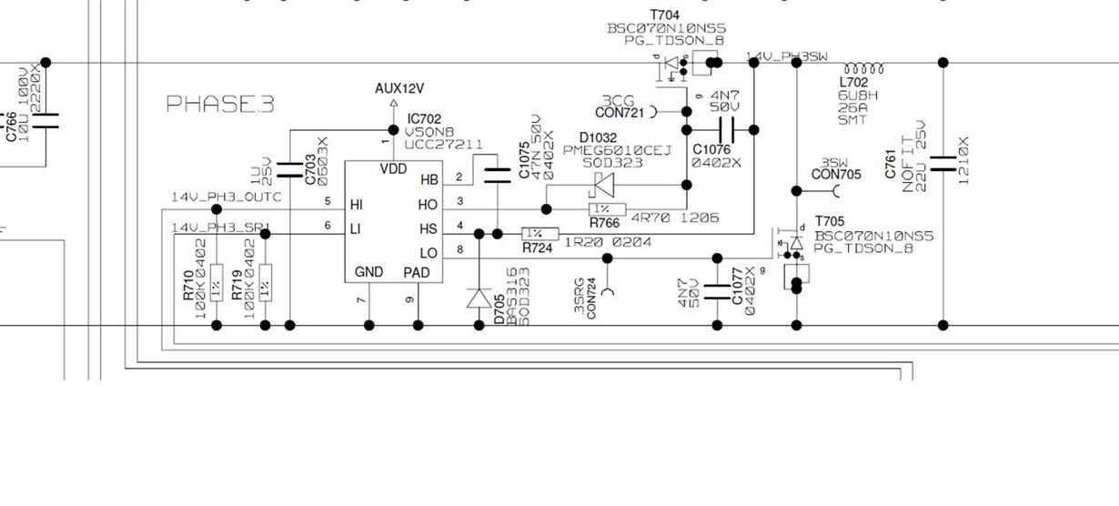
The converter is operating at 200KHz, I have included the relevant part of the schematic below:


Rg-on= R766+R724.

Rg-off= R724. D1032 bypasses R766 during turn off.

R724 and D705 is used to attempt to protect the HS pin from -ve spikes.

C1076 and C1077 reduces ringing on the gate, gave a slightly better gate waveform.

C1075 is the bootstrap capacitor.

T704 is the conduction mosfet.

T705 is the synchronous rectifier.

L702 is the output inductor, there are some electrolytic and ceramic capacitors as output capacitance not shown in this schematic.


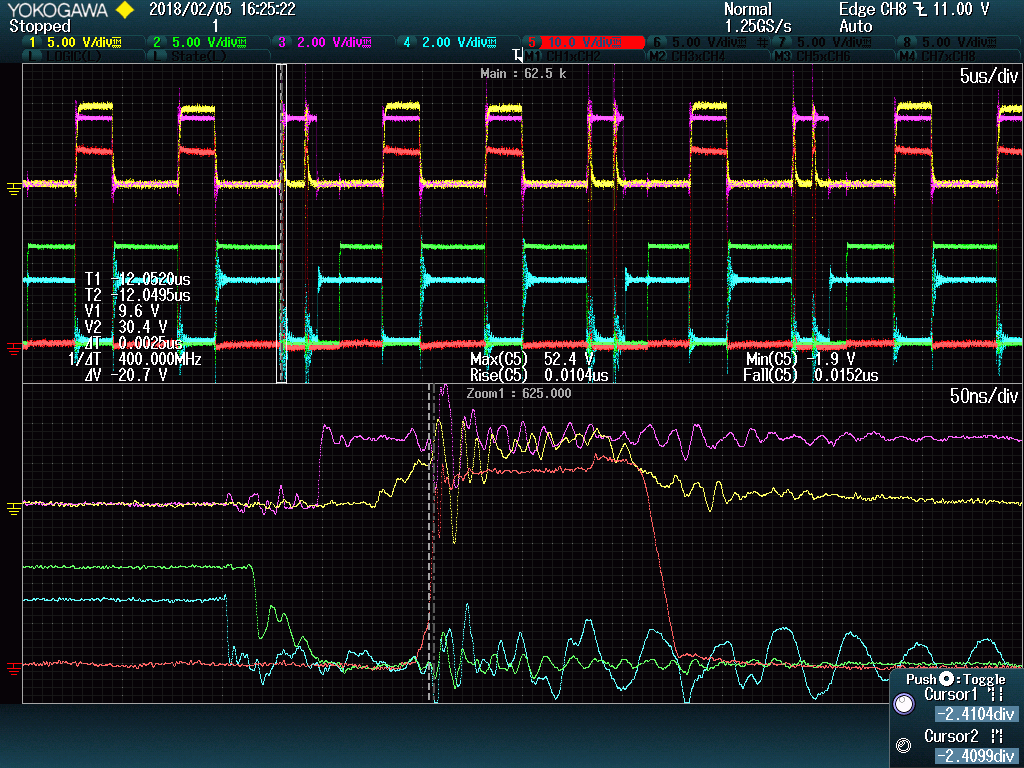
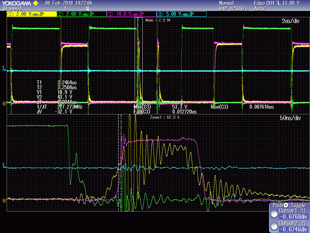
The problem is captured on the oscilloscope trace attached.
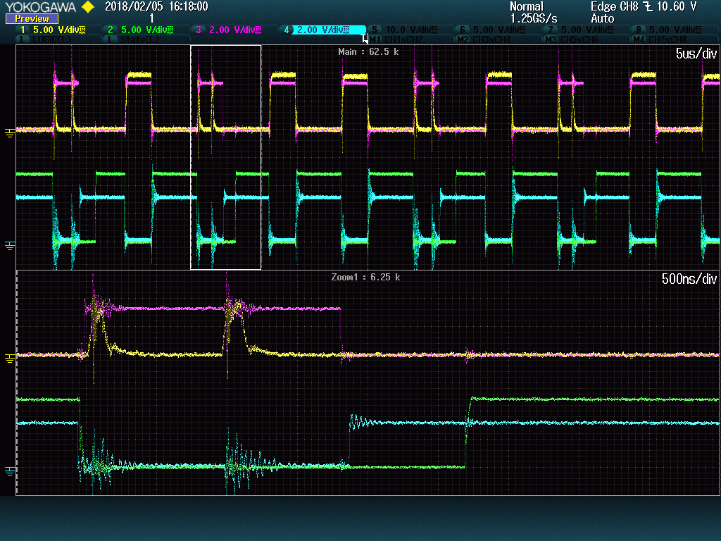
CH1=HO of UCC27211

CH2=LO of UCC27211

CH3=HI of UCC27211

CH4=LI of UCC27211


The fault happens once every 3 to 5 pulses. Basically when it receives a HI signal, it will attempt to turn on HO, but will then turn off, reattempt to turn on, then turn off again. And when its time for the Lower switch to go hi, it will have a delay before LO turns on.


I have checked the VH pin dv/dt during the fault, and it is about 8.28V/ns (which is within 50V/ns).

CH1=HO of UCC27211

CH2=LO of UCC27211

CH3=HI of UCC27211

CH4=LI of UCC27211

CH5=VH voltage


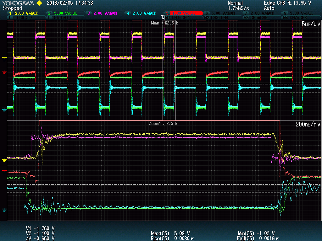
I have checked the VH pin Vmin during fault, and it is about -1.1Vmin (which is over -1V), however the HO pin goes down when VH is positive. CH5=VH voltage
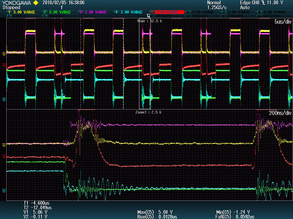


I have then checked the VH pin Vmin when there is no fault at ambient temperature, and it is very similar. CH5=VH voltage.


I have checked the VDD pin during fault, and it is 10.2Vmin (which is above UVLO). CH5=VDD


I have a possible solution to this problem by adding an RC snubber on the switch node, this seem to helped with the problem since it is much more difficult to induce the fault with the snubbers on.


I am wondering if a product expert can give me some advice on what they think the problem is inside the gate driver.

Why it is shutting down the HO and also delays the turn on of the LO every time the fault occurs.

As far as I know, the UVLO of HS only affects the high side. I cannot see it is the UVLO of the low side from the scope measurement.

What is the time for the gate driver to recover from an UVLO fault, this can allow me to check if the timing corresponds to a UVLO trip.

The dv/dt of the VH pin is well within its rating, however I do manage to fix it by adding a snubber to slow down the switch node.

This leaves only the VH pin negative rating, but the negative spike is very similar at ambient temperature under normal condition, and I’m not sure whether it will affect both HS and LS outputs.


Any advice would be very much appreciated.


Thank you.


Kind Regards,

Raymond

  • Hello Raymond,

    Thank you for your interest in the UCC27211. I am an applications engineer with TI High Power Driver group and will help to address your concerns.

    The schematic and scope waveforms is helpful information to help with the concerns. I do have some information that I want to confirm from the schematic and waveforms.

    Based on the LO waveform on the 1st scope graph it looks like VDD is ~12V, LI and HI is ~3.3V pk. Can you confirm?

    Also on the schematic I see the power MOSFET as BSC070N10N55. I was not able to find that exact number datasheet, is this the BSC070N10NS3 or similar?

    On the 3rd scope plot where you show the VH voltage at 1V/div, is this the VHB-VHS high side bias? Can you confirm the measurement of VH, differential or to ground, and which pins on the IC?

    Based on the behavior of the HO output this could be caused by a UVLO on the HB-HS high side bias. The UVLO delay times can be within what is shown in the scope plots, it is dependent on the two levels of the voltage on the HB pin (high and low level of the ripple).

    If the VH voltage on the 3rd plot is the VHB-VHS bias ripple voltage, this does appear to be fairly high ripple. The placement and layout of the VDD capacitor and VHB capacitor is important for proper operation. Ensure that the VDD capacitor is placed close to the IC and connected to VDD and VSS pins with short traces as possible. The same advice for the VHB to VHS capacitor, place close to the IC as possible and connect with short traces. As a troubleshooting measure, can you test with the C1075 (bootstrap capacitor) value of 100nF?

    In the scope plots there appears to be noticeable high frequency ringing on the LI and HI inputs, this may be due to noise induced in the probes. In the case there may be high frequency noise on the actual driver inputs I suggest trying adding small bypass capacitance to the input pins LI and HI. Try 22pF to 33pF placed close to the UCC27211 input pins and ground. High frequency false triggering can cause unexpected discharge of the bootstrap capacitor.

    It is not clear the cause of the LO delayed turn on at this point. Can you provide a scope plot of the HS pin voltage to ground both at a scale to capture the peak to peak, and an expanded scale to see the negative voltage to ground?

    Regards,

    Richard Herring

  • Hi Richard,

    Thanks for looking into this.

    I can confirm VDD is 12V and LI and LO are driven with 3V3.

    The power mosfets and rectifiers are Infineon BSC070N10NS5.

    On the 3rd plot is actually the HS voltage w.r.t. ground (i.e. VHS to GND). I didn't use a differential probe, I used a 500MHz probe with a very short ground wire (close probe technique). The measurement was taken across D705 diode which was placed about 2mm away from the UCC27211 IC. My aim was to accurately check the negative voltage of HS pin to ground.

    The VDD capacitor (C703) and the bootstrap capacitor (C1075) are placed very close within 2 to 3mm of the IC.

    I had tried increasing the VDD capacitor C703 from 1uF to 4.7uF, but I can still repeat the failure.

    I had tried increasing the bootstrap capacitor C1075 from 47nF to 100nF, but it also can still repeat the failure.

    I have not tried putting 22pF to 33pF on the input signals yet, I will try and do this next.

    The previous scope traces are the HS pin voltage to ground (CH5). The 2nd scope trace shows peak voltage of HS pin is about 52.4Vmax. The 3rd scope trace shows min voltage of HS pin to ground is about -1.24Vmin.

    Thank you.

    Kind Regards,

    Raymond
  • Just an update: I have tried placing 33pF on the input signal HI and LI, but I can still repeat the failure.

    Do you think high dv/dt noise will likely coupled into the UVLO circuit?

    And would you expect an -ve voltage over the rating of the HS pin will have caused the problem I am seeing, or is it more likely it will a catastrophic damage to the IC?

    Thank you.

    Kind Regards,

    Raymond 
  • Hello Raymond,
    Thank your for the update. Noise on the driver inputs is a common cause of driver output unexpected behavior so the filter cap on the input pins is usually worth investigating.

    It is possible that depending on layout trace length, and parasitic inductance that there can be high frequency content on the driver VDD-VSS and/or HB-HS pins which may trigger UVLO. To confirm this please confirm if the VDD capacitor is placed close to the IC and has very short trace lengths to the IC pins, Also confirm the same with the HB-HS bootstrap capacitor. Try moving the VDD cap and HB cap as close as possible to the IC pins as an experiment.
    Bypass caps for VDD and HB-HS should be good quality ceramic with X7R being recommended. To attenuate HF signals, it is often recommended to add a parallel ceramic capacitor of 1000pF which has a much higher frequency self resonance.

    Regarding behavior with negative voltage on HS, misbehavior of the driver output state can occur with excessive IC pin undershoot, not necessarily resulting right away in IC failure.
    I see that R724 and D705 should limit the negative voltage on HS. Confirm that D705 is located as close as possible to the IC pins. Also can you confirm the negative voltage level on HS, and that it meets the datasheet limit of -(24V-VDD) for <100ns?
    Another experiment to try regarding overshoot and undershoot on the driver pins is to add small 1A schottky diodes to clamp LO to ground and VDD, and HO to HS and HB. Use small package devices close to the driver IC pins. Connect anode of one diode to LO and cathode to VDD, connect anode of another diode to VSS and cathode to LO. Connect the diodes to HO, HB and HS in the same configuration.
    This will help determine if driver output overshoot or undershoot may be the issue.

    Regards,
    Richard Herring
  • Hi Richard,

    Thank you for the response.

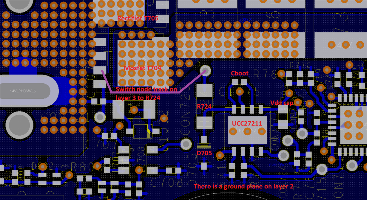
    Below is the layout, Vdd cap and bootsctrap cap are pretty close to the IC:


    I will try adding diodes on the HO and LO outputs next.

    With regards to UVLO fault, can you tell me a rough figure of the recovery time for the device (the time when UVLO is cleared to when the HO/LO outputs can trigger again) please.

    Thank you.

    Kind Regards,

    Raymond
  • Hi Richard,

    This is an update from further testing.

    I have tried placing a 1nF X7R 0402 capacitor in parallel with VDD cap, and also another one in parallel with the Bootstrap cap. However, I can still repeat the problem.

    I have tried placing PMEG6010 schotkky diodes to clamp HO to HB and HS, and also clamp LO to VDD and GND. However, I can still repeat the problem.

    I have capture some further scope traces of HS pin to GND.

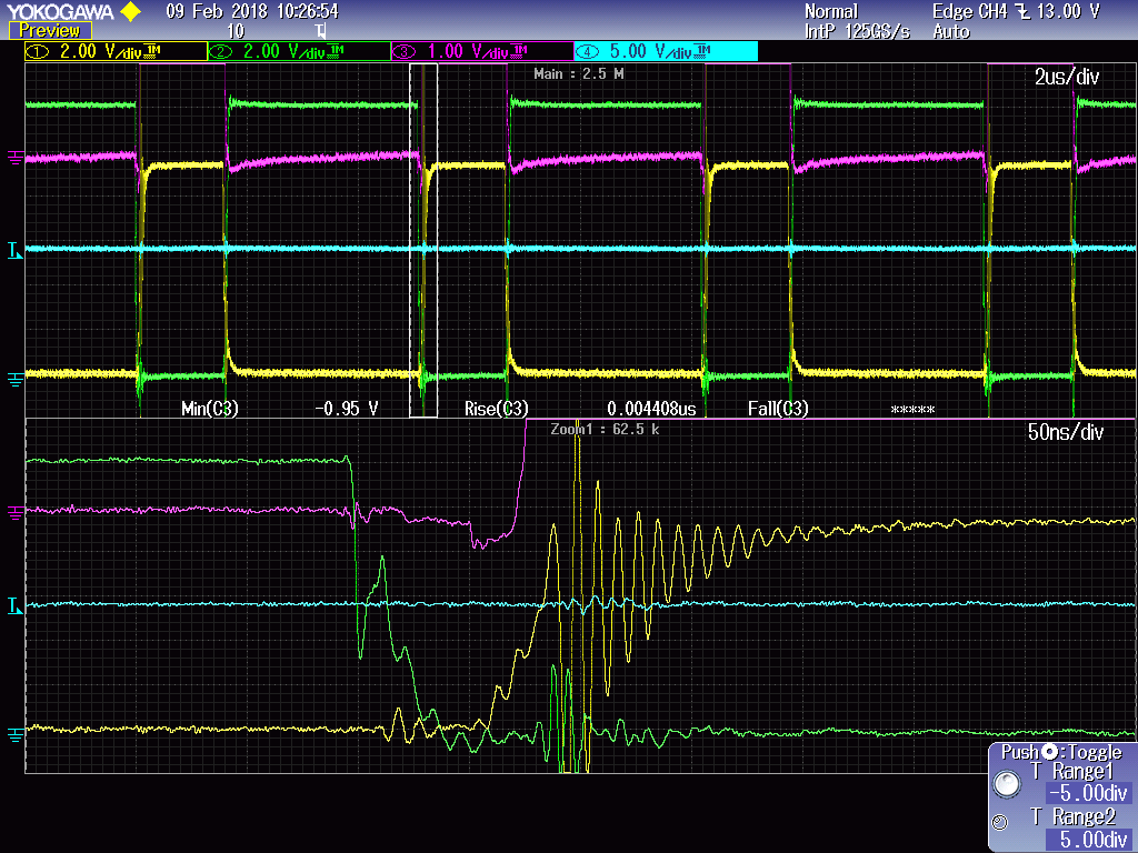
    Test @ ambient temperature without fault:
    CH1=Mosfet Vgs     CH2=Rectifier Vgs     CH3=HS voltage to GND (close probe technique)     CH4=converters Vout
    The zoomed in trace showed HS voltage Vmin=-0.95V for about 25ns during mosfet turn on. (You cannot see the entire voltage because I focused into the negative section)

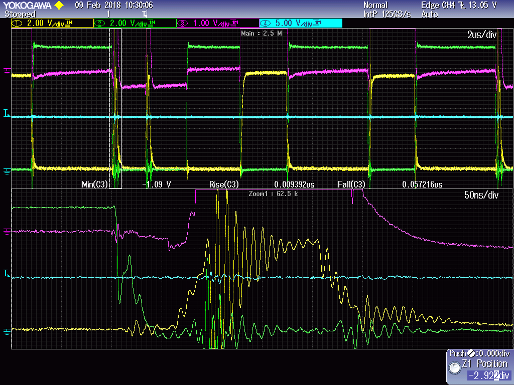
    I captured another trace during the moment I induce the problem by spray freezer spray over the circuit.
    CH1=Mosfet Vgs     CH2=Rectifier Vgs     CH3=HS voltage to GND (close probe technique)     CH4=converters Vout
    The zoomed in trace showed HS voltage Vmin=-1.09V for about 25ns during the turn on instance where the fault occurred.

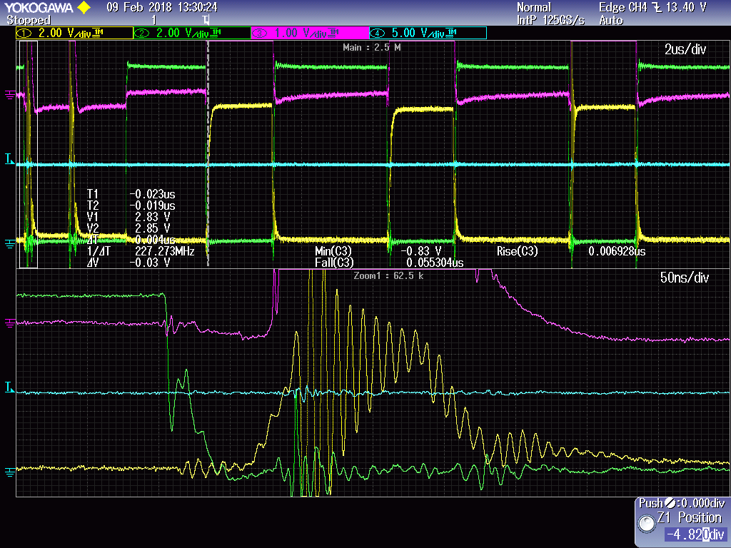
    As another test, I use a Schottky diode PMEG6010 (instead of BAS316) for D705, then capture another trace while inducing the fault with freezer spray.
    CH1=Mosfet Vgs     CH2=Rectifier Vgs     CH3=HS voltage to GND (close probe technique)     CH4=converters Vout
    The zoomed in trace showed HS voltage Vmin=-0.83V for about 25ns during the turn on instance where the fault occurred. Even though the negative voltage is within spec, I can still replicate the problem.

    It seems like the UCC27211 still misbehaves even when the HS pin voltage is within its negative voltage rating. It maybe that I cannot measure the negative voltage accurately, however I did see the negative voltage reduced with a schottky diode as expected.

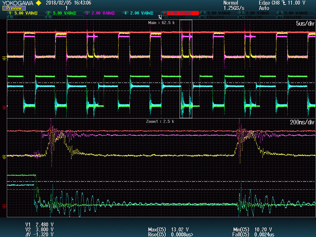
    The next assumption for root cause may be the dv/dt rating of the HS pin. I had captured the Switch node dv/dt during the problem.
    CH1=Mosfet Vgs     CH2=Rectifier Vgs     CH3=HS voltage to GND (close probe technique)     CH4=converters Vout
    Using cursors, I measure the dv/dt of the turn on to be 32.1V/0.0044us=7.30V/ns. This is within the rating of 50V/ns.


    During ambient conditions when there is no fault, the dv/dt of the switch node is a little slower at about 5.64V/ns.
    Freezing the circuit speeds up the switching.

    To resolve the problem, I added a RC snubber to the switch node which slows the dv/dt down to about 3.80V/ns.
    The snubber did not reduced the negative voltage on the HS pin, it is -0.95V without snubber, and with snubber it is -0.96V. It is effectively the same.

    I took a look at TI's training video (link attached below), and they said hi dv/dt can cause malfunction. I wonder if you think this is the same issue as describe in the video and maybe if you know any further details of the root cause of the malfunction. It is talking about another IC, but I am not sure if the UCC27211's internal circuit is similar to this. For your information, I did not separate GND and PWRGND, I use a big ground plane for all grounds.

    https://training.ti.com/gate-driver-training-series-gate-driver-operation-high-dvdt-and-didt


    Thank you.

    Kind Regards,

    Raymond
     

  • Hi Raymond,

    I will be filling in for Richard since he is OoO.

    Are you keeping the input filters on throughout this testing to clean up the noise coupled back to input from the switch node? Maybe we need to combine all the fixes into one (find the best fix - then put the snubber and filter back on for an even better fix). Since this is a buck converter the inductor current closely mirrors the load current, and with a higher load current the gate drive charging loop and the output filter loop share the switch node at the same time increasing the possibility of parasitics interacting, some of this noise can be filtered at the output as well by using low ESR MLCC types and multiple capacitors of different size. This will clean up the GND and HS reference as recommended from the training.

    For the UVLO there is a Symmetrical UVLO Circuit that Ensures high-side and low-side shut down at the same time. For VHB UVLO only the high side is disabled. I will find out what the UVLO fault recovery time is and let you know.

    Since you are measuring far from the max slew rate of 50V/ns on HS then this doesn’t seem like the problem however looking at your scope shots its contrary and could be violating this spec with all the unwanted ringing. The issue happens when the high side turns on, in which there is little ring on HS compared to Vgs however the HS rise is non-monotonic this seems to be a good focus to start the root cause. Can you slow the rise time with a larger gate resistor value and see what happens? If we can slow the dv/dt on HS down then we should be able to prevent ringing on HS node from reaching HS reference pin triggering the subsequent missing pulse. Another way to experiment is to lessen the drive capability of the bootstrap cap by decreasing the value of this cap and therefore reducing the current the cap can supply (but not necessarily reducing the dv/dt that this may also endure).

    Thanks,
  • Hi Jeffery,

    Thank you for looking into this.

    I have done some more testing by lowering bootstrap capacitor from 47nF to 22nF as you suggested, but I do not see much difference in waveform and I can still replicate the problem.

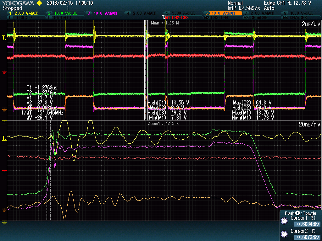
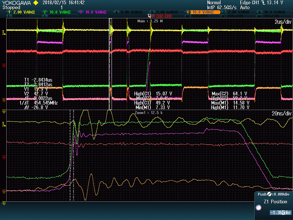
    CH1=Vo,  CH2=HB wrt ground,  CH3=HS wrt ground,  CH6=Vgs of mosfet,  M1= maths function CH2-CH3 ie:HB wrt HS.
    I used non-differential passive probed with small ground wire (close probe technique) to measure HB and HS, hoping to get rid of all measurement noise.

    The shot below is with 47nF bootstrap capacitor, it was triggered during the fault when I spray it with freezer spray.
    The HS dv/dt = 26.1V/2.2ns=11.86V/ns.
    The HB-HS Vmin= 7.33V.
    I believe this is within the UVLO threshold for the upper gate which is 7.9V-1.1Vhyst=6.8Vthreshold.

    The shot below is with lowered 22nF bootstrap capacitor, it was triggered during the fault when I spray it with freezer spray.
    The HS dv/dt = 26.8V/2.2ns=12.18V/ns.
    The HB-HS Vmin= 7.33V. This is again within the UVLO threshold.

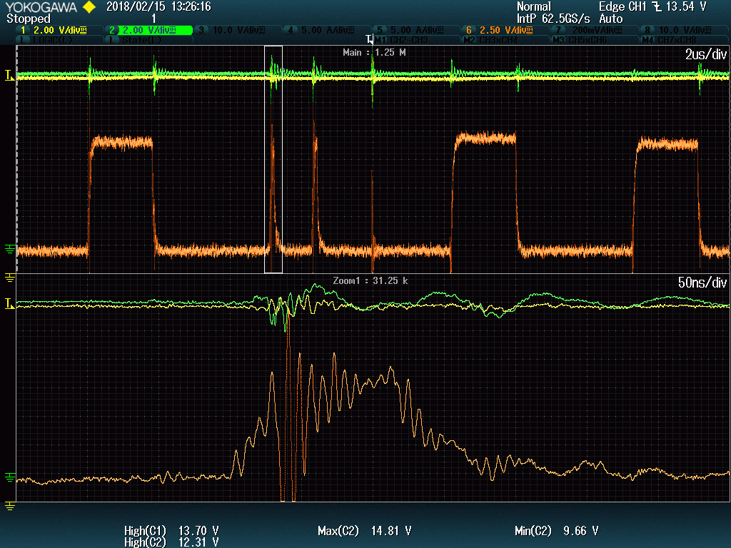
    I have also use close probe technique to look at the VDD capacitor voltage during a fault, but VDD-min=9.66, so it is above the UVLO threshold.
    CH2=VDD

    I will now show you the difference in dv/dt of the switch node before and after I added a RC snubber on the switch node.

    This is the waveform with the snubber added:
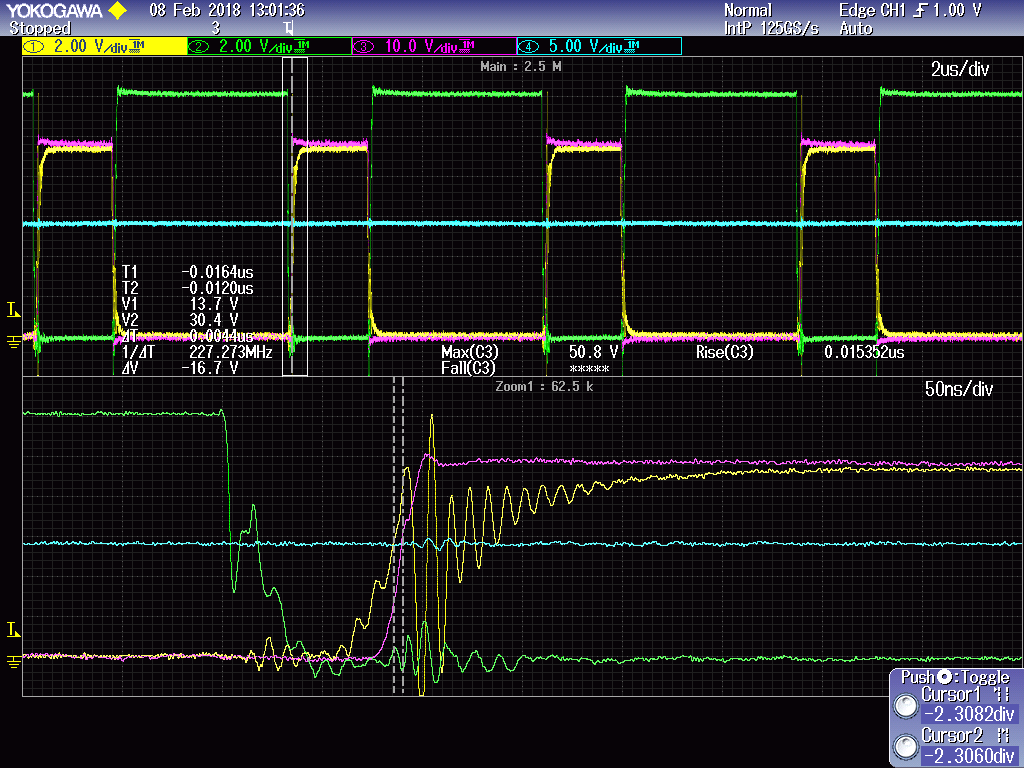
    CH1=Mosfet Vgs,  CH2= Rectifier Vgs,  CH3= Switch node (Rectifier Vds), CH4=Vo
    Switch node dv/dt=16.7V/4.4ns=3.80V/ns, rise time=0.015us.

    And this is the original circuit without the snubber:
    dv/dt=24.8V/4.4ns=5.64ns,  rise time=0.01212us.
    As you can see, the original switch node waveform has a slight extra ring near the top, but I am not sure if this will cause a problem

    Thank you.

    Kind Regards,

    Raymond
  • Hi Raymond,

    Thanks for your reply. This issue appears to be a noise issue on HS and more important HI/LI. Are you able to retest putting more capacitance on HI and LI, say 470pF or 1000pF to get rid of some of the noise in order to further troubleshoot?

    Thanks!

  • Hi Jeff,

    I have re-tested with added 1nF on HI and LI, but I can still replicate the fault.

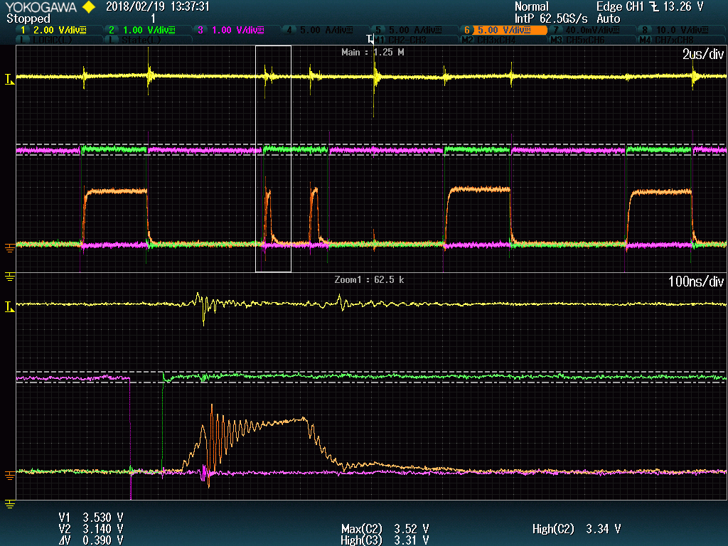
    I have taken scope shots of LI and HI using close probe technique to get rid of measurement ringing.

    Original circuit without adding 1nF:
    CH1=Vo, CH2=HI, CH3=LI, CH6=mosfet Vgs
    Using close probe technique, no ringing seen even without 1nF. HI Vmin about 3.14V.

    I've then added 1nF just to verify that I can still replicate fault:
    HI and LI ramps up slower as expected, still no ringing, but can still replicate fault.

    I believe we can rule out HI and LI noise issue.

    Thank you.

    Kind Regards,

    Raymond
  • Hi Raymond,

    Thanks for your update, we can rule out the noise. For now, lets assume that the device high side output HO is in UVLO. This would be happening due to an overshoot on HS making HB-HS dip below UVLO threshold. If this is the case lets first look at the boot 47nF and gate/source 4.7nF cap. Are these caps NPO or X7R? Can you try reducing the 4.7nF gate to source cap and/or increasing the boot cap, test each separately to see the effects, then concurrently to see how it helps.

    Thanks,

  • Hi Raymond,

    Any update with the issue? if you resolved this can you share what your solution was?

    Thanks,