This thread has been locked.

If you have a related question, please click the "Ask a related question" button in the top right corner. The newly created question will be automatically linked to this question.

UCC28950-Q1: Synchronous Rectification error

Part Number: UCC28950-Q1
Other Parts Discussed in Thread: UCC28950

Please could somebody support with the following error I notice especially at low DC Input voltage and whilst SR is active.

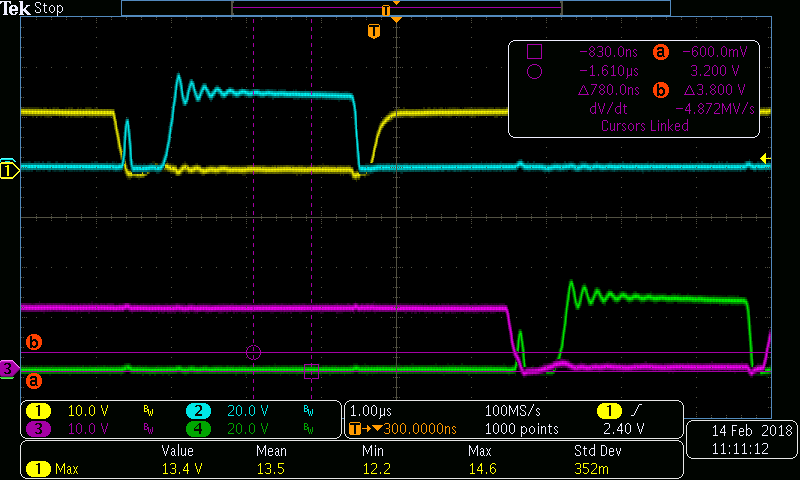
During the switch OFF period I notice a pulse in the Drain waveforms of E+F whilst monitoring gate waveform of each ( attached image ). Has this issue been encountered before?

  • Hello Mark

    This may be due to loss of ZVS on the primary.Can you check the Vds waveforms of the low side FETs and also their Vgs waveforms.

    Loss of ZVS can be seen in a very high dv/dt rate at he FET drains as they begin to hard switch. You should also see a miller plateau on the Vgs waveform if ZVS has been lost.

    Can you quantify what you mean by 'low voltage'

    Please feel free to post the waveforms you take and I can review them.
    If ZVS has been lost then the solution is probably to increase the amount of energy available to drive the primary switching transition - or reduce the stray capacitance at the switched node so that the available energy is sufficient.

    It may be that loss of ZVS doesn't incurr too much of an efficiency loss penalty, in that case the behaviour you are seeing may be acceptable in your particular application.

    Regards
    Colin
  • Good Afternoon Colin

    Many thanks for the quick response..

    Currently testing at 168vdc input volts ( however this pulse is appearing at higher volts but lower amplitude)

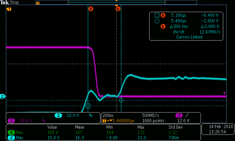
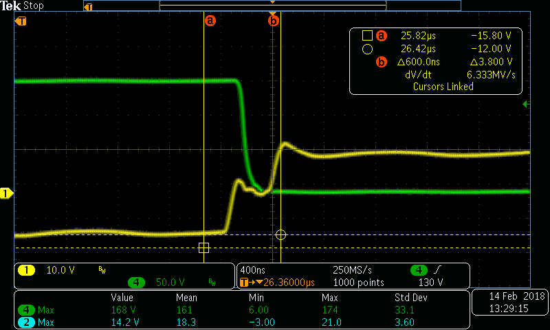
    I rechecked ZVS operation , looks OK to me at AB / CD gate>drain checks (attached)

    Efficiency however is actually OK....

  • Hi Mark

    I'd agree with you that the primary circuit is achieving ZVS.

    One other thing to look at is whether the output inductor current is negative (flowing from drain to source) when the SR is turned off. One relatively easy way to check this is to vary the load current. As the load current reduces the minimum value of output inductor current may become negative - although the average value remains positive. If this is the mechanism then you should see the spikes disappear as the current is increased.

    You are using the UCC28950-Q1 and the SR drives may be turned off at a pre-determined current by setting the voltage at the DCM pin according to the instructions in the DS.

    Let me know how you get on.

    Regards
    Colin
  • Hi Colin

    Many thanks for the fb , I will look into this again next week.

    One point I would like to ask , I currently use a shim inductor and would like to know if there are any benefits or negative side effects for placing in the CD node rather than AB - any thoughts?

    Best Regards

    Mark

  • Hi Mark

    That's an interesting question.

    Redl et al in the IEEE publication 'Switch transitions in the soft-switching full-bridge PWM phase-shift DC/DC converter: analysis and improvements' Published in: Telecommunications Energy Conference, INTELEC '93. 15th International

    They state that the both positions are equally effective in clamping the transformer voltages BUT the diode currents are different. They recommend placing the inductor in the AP (Active/Passive) leg - that is in the CD leg using the normal TI convention.  They benefit is reduced dissipation in the diodes but - if I read the paper correctly - the total system current is unchanged and the reduction in diode dissipation is accompanied by an increase in dissipation in the MOSFET body diodes. Unfortunately I cannot share a copy of the paper with you but you may be able to find it on the internet.
    In a practical sense our UCC28950 EVM places the shim inductor in the PA (Passive/Active) leg - that is the AB leg in 'TI-speak'. Most of our customers do the same although I know of at least one who places it in the CD leg.
    Regards
    Colin
  • Hi Colin

    Many thanks for the detail , I will be keeping with AB leg method.

    One more point , I have a 3kw Master / Slave setup and wondering if any guide exists especially for the layout consideration?

    Regards

    Mark
  • Hi Mark

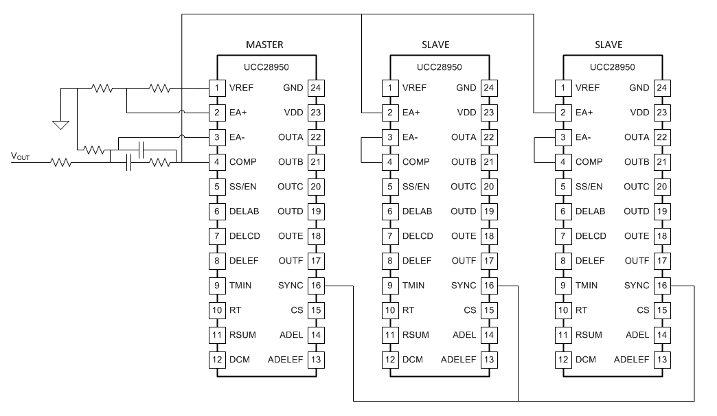
    This diagram below shows in general terms how to set up a Master Slave arrangement with synchronisation using the UCC28950. Synchronisation is actually optional here but it makes some sense because it will reduce the audible noise from the beat frequency that you will get from two unsynchronised oscillators. The switching noise will also be synchronous which is useful because any switching noise which is being cross coupled from one power stage to the other will always appear in the same place on the CS ramp and be less likely to cause unwanted duty cycle jitter due to noise spikes on the CS signal. The SYNC signal is also a relatively high amplitude digital signal and easily transportable from master to slave without excessive distortion.

    The COMP output from the master must be daisy chained across to the slave. Depending on the physical distance between the two controllers you may need to do one of the following

    Simply connect the COMP from master to slave.

    Add a buffer at the master COMP output connect across to the slave.

    Use a fully differential connection - COMP and GND - to bring the COMP signal over to the slave

    I'd use a high frequency RC filter at the slave in all cases

    There isn't a document describing layout considerations but the first step if recognising that layout is important and of course careful attention to the layout to minimise noise pickup from the power stage is needed. You need to be able to ensure that the GND references for both master and slave are actually at the same potential - or use a differential connection for the COMP signal. Ground planes work well to reduce E field noise but are not effective for H field interference so keep signal lines away from sources of H field (transformer and inductors). Ground planes should not have slots in them and if they do then signal traces should be routed around the slot - that is the signal lines should be tracked over the ground plane copper. Keep the SYNC signal, and the OUTx signals away from the CS signal. Don't run the SYNC or OUTx signals under the IC body (unless there is an intervening ground plane)

    I'd be happy to review any layout that you are considering -


    Regards
    Colin