This thread has been locked.

If you have a related question, please click the "Ask a related question" button in the top right corner. The newly created question will be automatically linked to this question.

UCC28711: UCC28711

Part Number: UCC28711

I designed a DC/DC converter , 220V-550Vdc to 8Vdc. . Min load is 130mW, max load is 4200mW.  The converter runs in burst mode up to 1.2W ( high ripple). I need to be in continuos mode at min load  because the ripple in burst mode is not acceptable.  How can I achieve this task  ?

Transformer primary ind is 6mH, Np-s=16.666 ( primary to sec), Np-a= 10.9375 ( primary to aux), Ns-a= 0.65625 ( sec to aux)

Aux_PS_Sch.docx

  • Hey Aurora,

    The UCC28711 does not have burst mode, you may be hitting a protection fault causing a reset cycle.

    If you can provide wave-forms of the output voltage, VDD of the chip, and the waveform across the current sense resistor connected to ground, we may be able to pin-point what is going on.

    Also, is it possible to get a clearer schematic that would help me out.

    Regards,
    Davit
  • Please see attached the schematic. Tomorrow I will send you the required waveforms.

    Aux_PS_Sch1.docx

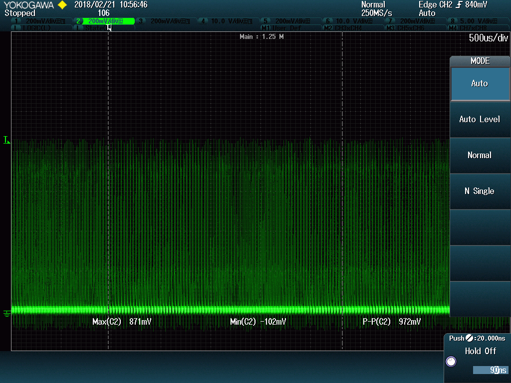
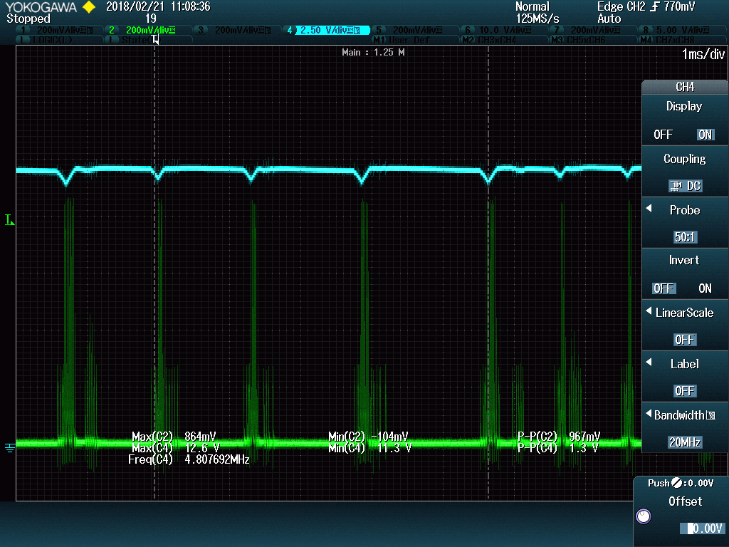
  • Attached waveform  6  and 7 of CS pin ( ch. 2) and Vdd ( Ch 4). No 6 shows power over 1W ( working well) and no 7 shows  min load , 200mW power( high ripple - not aceptable).

    Can I put 10nF cap on CS pin?  What about Vsense ? Can I use 1k ( R13) and 47pF from Vsense to return ?


  • Hey Aurora,

    A 10nF capacitor on the Current Sense pin would be too large. It is recommended actually to not have any capacitors on the pin, as it would lead to filtering information and cause a reaction delay due to the added RC constant. It should not be necessary to place a capacitor on the CS pin.

    For the VS Pin, do not place a capacitor for reasons similar to the CS pin, but also because the VS pin is time sensitive and any delays may affect proper operation of the device. What are the intentions with placing a resistor in series with the VS Pin?

    At what input voltage where these waveforms taken? I ask because the RLC resistor may be over-compensating at high line causing the device to operate in the way you see it.

    Regards,
    Davit
  • The waveforms are taken at 220Vin . 1nF to 10hF cap on CS pin helped  ( made the converter a little more stable) but it did not solve the issue.  I asked about VS  pin hoping I might be able to put a filter, 1KR resistor with 47pF.   I know that the pin is very sensitive. I can not even probe it with a scope unless I have 1KR resistor between the pin and the signal . 

    Anyway, do you have any suggestion how to solve the issue without adding caps or 1W  pre-load ?

    Best Regards,

    Aurora

  • Hey Aurora,

    One guess is that your snubber may be oversized for the light load operation. If the snubber is oversized, then during the light load operation, it will be a parasitic load, since the capacitor will have to be charged every cycle since during the off time or when the controller is off it is being discharged by the resistors. I think one thing you can try is to increase the size of R1 and R2, or, if the TVS is sized correctly for full load, just use that snubbing system instead.

    Is there a reason why you have an RCD snubber and a TVS in parallel?


    Regards,
    Davit
  • Hi Davit,
    Sorry for the confusion. Only RCD snubber is fitted. The other option (with TVS) is not populated.

    Regards,
    Aurora
  • Hi Davit,
    Can I have any load on V_aux ? let's say 25mA.

    Best Regards,
    Aurora
  • Hey Aurora,

    You can have a load on V_aux. The issue then becomes cross-regulation.

    For low load, 130mW, your secondary side output is a load of 8V, 12.26mA. Your auxiliary winding power (12V, 25mA) is now more than your secondary side power, leading to the controller regulating the auxiliary winding rather than the secondary side winding.

    Regards,
    Davit