This thread has been locked.

If you have a related question, please click the "Ask a related question" button in the top right corner. The newly created question will be automatically linked to this question.

UCC27714: LO side driven Cboot oscillations HO output

Guru 54087 points
Part Number: UCC27714
Other Parts Discussed in Thread: TIDA-00778

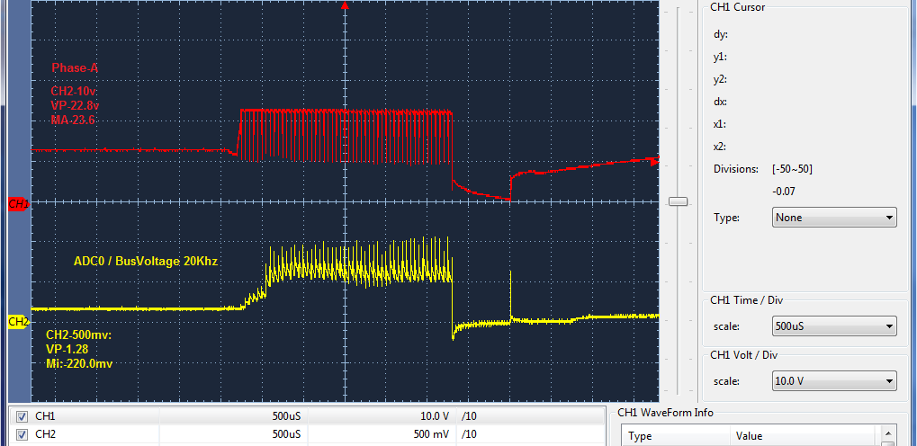
Very strange issue proven software other vendors gate drivers does not cause large voltage surge during Cboot charge cycles. This issue refers to 3 phase commutation and 24VDC bus supply rising to over 90vdc with inverter loaded or not. A custom PFC was resolving 80v-90v PWM surges controlling DC bus voltage. That was the only way Cboot cycles could ever succeed let alone FOC commutation drive a connected motor to 7600RPM.

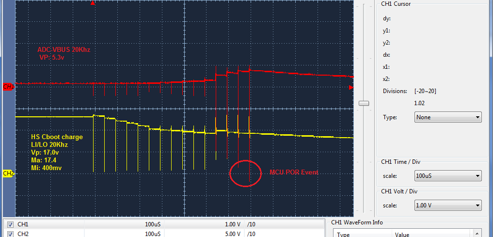
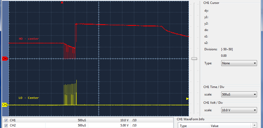
The PWM frequency 20Khz driving 500ns Cboot duty cycle (1%), user settable charge time 1-255ms. Capture below taken single phase (1/2 bridge), all phases resemble similar pattern though signals cut off in 2ms when PWM fault handling has been enabled. Otherwise the 500ns Cboot pulses POR the MCU very abruptly.  UCC pin 4 (EN) was kept high 3v2 (enabled) at all times of this testing.

How could HO drives stay on during Cboot cycles when the MCU PWM control block keeps all 3 HI (low) during Cboot cycles? Do we not expect H0 side should always be low during Cboot cycles or have I missed something in how 1/2 bridge shoot through occurs? Perhaps these 3 gate drivers are messed up in some way and do not follow proper 1/2 bridge switching conventions. The LO side gate drives pulse rising edge from ground producing the odd wave form below. The LO side seems correct in my opinion but not HO staying active during Cboot cycles so the HO single is some how being inverted.

CH2: ADC0 channel input reporting DC voltage. Signal represents 70-80V peaks from 24VDC supply low/left side of signal prior to undesired POR of MCU, far right.

  • Hi BP101,

    Thanks for your question.

    So before switching, it looks like your Phase A Switch node is floating around 13V as we saw previously. It then goes up and clamps to 24V as you switch the low side, then bounces between 24V and ~10V till forced MCU POR.

    I'm interested in seeing the HO-HS voltage during this event, at a smaller time scale where we can see individual switches. Also, could you post your drive-side schematic with bootstrap cap and resistor values?

    Best Regards,

    John
  • Hi John,

    Might I PM the whole schematic PDF so you can see the VDD supply too?

    I was able to tweak pre-charge pulse width, produce 105ns falling edge pulse aimed toward ground. The HI drives are kept false and all three phases LO pulsed 105ns. The original pulse width edge fell near 50ns and never caused this issue, fact I caught UCC produce 50ns pulses 1 time only. The odd part is the UCC would not repeatedly produce 50ns pulses. Hard to imagine the UCC is behaving so badly when most all design precautions were followed. Also tried to produce a wider pulse (200ns) but it seems more destructive. Seem to recall 30ns pre-charge pulses were being produced in the past when 12.5Khz pre-charge pulse width set 1% PWM duty.

    So why has UCC been restricted to 100ns LO and still function in TIDA-00778 is more the question. The disruption in the 24v switching power supply from even 100ns pulses the TIDA engineer should have reported, less he simply tested with linear 300vdc supply? Never should first test PWM drivers at high voltage prior to low voltage testing in any new design, would have revealed such looming disaster as I report here. The amount of DC supply bus disruption in that Cboot charge cycle is abhorrent! Even parallel 680uf caps can't stop the impending surge.

    Odder yet a 50ns pulse width produces the same 100ns pulse when LO/HO should ignore the pulse entirely according to datasheet. Hard to imagine the ADC 24v Bus voltage rings negative from 220mv to roughly -6v after changing pre-charge pulse width 100ns to ground. MUC often POR's immediately upon the 100ns return to 13v.

    Part values are based TIDA-00778 and application section of datasheet, Rboot 3.3ohm, Cboot 1uf.  

  • Surges  occur either way the pules are created from 24v -13v or 24v to 0v. UCC don't  produce a pulse less than 150ns in repetition in the first few pulses it seems. The period is set at 50us, the pulse width (3000/245*60Mhz) or 0.2us and past (3000/100+1*50Mhz) was supposed to produce a  1% duty at several different PWM frequency according to source code text.

  • Hi John,

    Sorry to inundate with so much info, perhaps you guys have a better way to pre-charge Cboot that does not cause so much spiking of DC Bus voltage? The capture pre-charge is set for 20ms but never gets that far before MCU POR event stop it dead. The red trace is monitoring 24VDC bus voltage through 120mohm ferrite bead series to BusVoltage: +24v_(o)_510k - 510k -----trace---- 6.8k to ground, 0.1uf ceramic cap to ground decouples near the MCU. Not sure why yellow spikes start to rises near the time of POR event but the negative red spikes are killers. 

  • BTW: Gate drive captures above HO is not instructed low by MCU, it is being discharged by LO instructed low by MCU and current path high side FET 20k gate to source. Had to think about that after wondering, what is going on there.
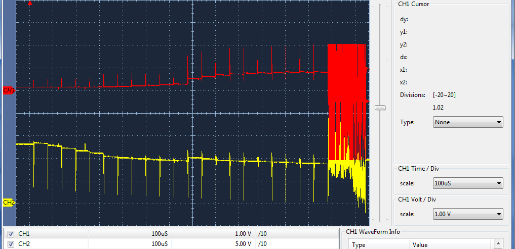
  • Below is another odd capture, note the sporadic oscillations occurring @500kHz near the end just as MCU has POR event. Have to wonder if HO/HS 20k shut off resistor is causing this since it is not on the FET gate. Required for parallel FET's a 20k shutoff is placed across UCC pins 11,12 with a 16v zener parallel to 20k limiting GS voltage below FET 20v Max. Tina PWM transient analysis of the parallel FET did not indicate such oscillations when short PWM duty cycle was being presented to HI/LI.

  • Hi BP101,

    Looking at the datasheet, section 6.6 Timing Requirements, the nominal Ton/Toff is 40ns, which may be the cause of the 50ns input and 100ns output. This was updated in Version B of the datasheet, though I do see confusion when looking at section 7.4.2 of the datasheet.

    With the sole intention of charging the bootstrap capacitor, might it be easier to switch LO on for approximately 15-20us (5*R*C = 16.5us) at startup? This should ensure adequate Cb charge time assuming 3.3Ohm/1uF values listed above. This also should be faster than running LO at 1% duty cycle/20kHz when it comes to Cboot charge time.

    Also, when HO is low, it is pulled to HS internally. When LO is high, HS is pulled to ground through low side FET - and HO follows. So HO pulls to ground through the UCC - not the 20k G-S resistor.

    Best Regards,
    John
  • John Geiger said:
    might it be easier to switch LO on for approximately 15-20us (5*R*C = 16.5us) at startup?

    Something else is causing the harmonic crash or self firing of the HO output, only during Cboot charge cycles as discovered. The LO was  staying low the entire charge period when PFC circuit was installed as described below. It is by pure luck that somehow PFC was mitigating the crash condition. I noticed the LO stayed low the entire charge period and could not understand how that was occurring at first.

    So it is ok to have 20k/zener directly on UCC pins, not cause parasitic oscillations? That part of design is new and used to be on the other side of gate drive resistor in our prototype. Only moved it after Infineon technical brief on parallel FETS made a point to mention zener placed directly on gate lead can cause oscillations. Location seemed ok since Tina transient simulation plots of inverter PWM did not indicate oscillations occurring but duty cycle was greater than 1% and fixed. Seem to recall larger charge pulse widths lead to excessive current draw in the first 5ms of Cboot charging especially at high voltage above 50vdc.

  • John Geiger said:
    When LO is high, HS is pulled to ground through low side FET - and HO follows. So HO pulls to ground through the UCC - not the 20k G-S resistor.

    Will that case current to blast through high side FET at any point during Cboot charge cycle as LO is pulled taken high by LI. Yet HI is held low by 20k pull downs and not being MCU controlled during Cboot charge cycles. Wonder if that is causing parasitic oscillations every time LO rises falls HO follows rises but should be under RS latch control, not HS. 

    So HI needs to be held low by MCU so HO can not turn (back on) as HS returns each cycle. That seems to infer the RS latch Q drive is not in explicit control of the FET gate.

  • Hi BP101,
    If PWM duty cycle is adjustable, could the duty cycle be extended at startup to charge Cb in least number of cycles? Hopefully should mitigate those spikes, or at least the number of them.

    Having the 20k/zener on outputs should be fine as long as your VDD stays below the zener reverse breakdown voltage. If your VDD is overshooting and causing excess current in the zener, this wouldn't be ideal. Larger PW shouldn't draw too much current as Cb should charge fairly quickly.

    Best Regards,
    John
  • Hi John,

    John Geiger said:
    Larger PW shouldn't draw too much current as Cb should charge fairly quickly.

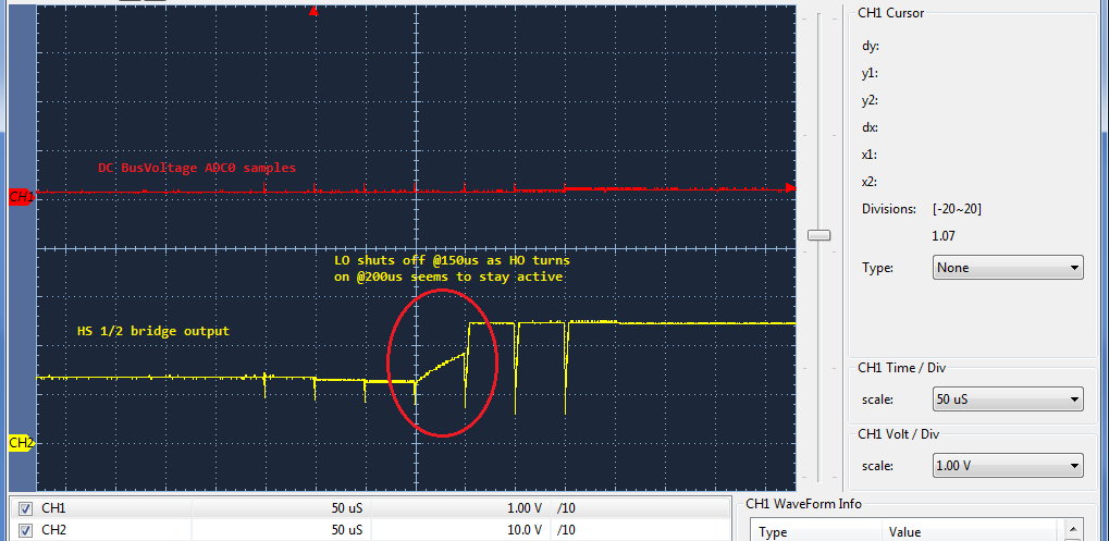
    Have tried to make pulses wider several times, HO still turns on after 150us as Cboot is charging when LO shuts off. It is obvious now that HO is somehow turning on driving the High side B+ to ground before MCU fault detection shuts it down. That is what is causing large spikes during Cboot at 150us from EN being enabled.

    John Geiger said:
    Having the 20k/zener on outputs should be fine as long as your VDD stays below the zener reverse breakdown voltage.

    The zener VzMax is roughly 16.04v and was relying on HO internal input resistance to limit current to 200ma @VR12ua and the VDD roughly 14.4v UCC pin  7 and

    Every time EN is lifted, after 150us Lo turns off and HO seems to rise from 10v up to 24v during Cboot charge cycles. That seems to drive high side FET to ground as LO shut off but it might just be the Cboot is fully charged after 150us? That behavior would seem at odds with how it always required 35ms or longer to get a full Cboot charge with other gate driver. The MCU fault protection is kicking in at 200us and charge period can go a bit further as capture above shows when Fault protection disabled. That was causes the 50-200KHz over voltage oscillations lock up the MCU even before open loop commutation begins.

    Either these gate drivers are bad for some unknown reason or some kind of errata has been discovered here. 

  • Seemingly good evidence HO is staying active as Cboot charges from LO pulses.  HS should then remain near ground and not return to B+ as it is doing.

  • Hi John,

    It seems the 3 gate drivers are fighting each other since HO appears to be directly effected by the magnitude of Cboot charge, Q thus seems to loose control of HO. That seems to point as a design issue of the UCC HO structure or all 3 drivers are defective relative to behavior of other vendors gate drives performance in the Cboot charge cycle.

  • Finally the center 1/2 bridge seems the culprit of the other two partners. Center 1/2 bridge is rising HO up to B+  during Cboot charge cycle for unknown reasons.  Previous captures were taken load attached, hindsight may have masked a 1/2 bridge faulting more often than the others.  Either way all 3 report over voltage faults even with no load attached may be due to this sudden jump of HO during Cboot charging.

  • Hi BP101,

    In this most recent capture, HO is seen to rise up to B+ (25V) after the 500 us Cboot charge cycle from the low side. Can you check each phase HO-HS differential voltage during this sequence to determine if one of the FETs is being switched, or if it is another current path? And yes, one phase could cause the overvoltage fault on the other phases assuming the motor is a Wye load, connecting the phases together.

    Best Regards,
    John
  • Hi John,

    Capture above is occurring on 2nd, 3rd UCC oddly not the 1st UCC, bridges are unloaded. It seems the Cboot charge cycle is acting as a voltage doubler and entering high frequency oscillations often elevate 24v to 90v or more from ground onto B+. The magnitude of HS voltage become worse when Cboot charge pulse width into HS is made wider, say 2us or more, a wider pulse LO turn on pulse exaggerates the condition.

    Somehow the UCC charge pump is acting like a voltage generator and not a floating (regulated) HO voltage clamped to VDD at all times. The charge pump floating voltage HO output becomes highly unstable when charging Cboot for what ever reason. I suspect parasitic oscillations are allowed to inflict the HO gate architecture and thus Q looses control of HO at very high frequency.

  • Hi BP101,

    What does the 1st UCC look like then? Is there any way you could take a capture at a smaller time scale when HO transitions from GND to B+? Also could you have the other channel monitoring HS?

    Best Regards,
    John