This thread has been locked.

If you have a related question, please click the "Ask a related question" button in the top right corner. The newly created question will be automatically linked to this question.

UCC27714: Distorted HO pulses / widths +/-1us often end up inverted or at a lower amplitude

Guru 54057 points
Part Number: UCC27714
Other Parts Discussed in Thread: TIDA-00778, ALLIGATOR

It seems we are unable to consistently produce a proper looking pulse width under or above 1us from MCU driven PWM generators as HI/LI are individually being delayed 40ns by UCC.

Previous system gate drivers only inserted delay matching on LO input and produced 8-80Khz PWM near 100% duty cycle on LI/HI via LO/HO. That is a joint effort requiring two UCC gate drivers and two synchronized PWM generators in Co-partner field phasing rolling into a third UCC for three phase commutation schemas. A-B, A-C, B-A, B-C, B-A, C-A co-partner hard switched half bridge schema requires 6 codes to drive inverter.  

Can the UCC by delaying separately LI & HI inputs 40ns maintain compatibility with TM4C1294XL PWM peripheral generators in co-partner phasing? From this point it seems the 40ns delay matching is obstructing proper pulse generation of co-partner gate drivers. When both HO/LO of co-partner gate drivers is required to develop such pulses, 1/2 the pulse generation is often MIA or being inverted upside down above supply rail, not always but more often than expected.

It appears the DC inverter in not keeping synchronous to the PWM generators at all times and produce very distorted pulses and widths in the process. Even the HO copartner that does not produce an inverted pulse at the end of each period is distorted and does not reach down to mid supply.

  • Below is input data to help those who have authority to check out why we are having such difficulty with UCC27714 gate drivers.

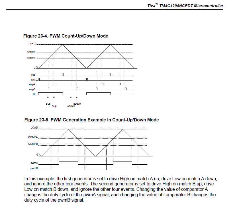
    TM4C1294 MCU PWM generator output pairs are illustrated below.

    Oddly 2nd/3rd UCC gate drivers produce runt pulses (>1us) pulse width and end up crashing copartner HO to LO transitions in the first 2500us of PWM generation with copartner (2nd UCC) driver. Oddly last two gate drivers producing runt pulses appear defective, driving HO to LO pulse generation down to mid supply. Only the first gate driver to receive PWM pulses with aid of copartner UCC seem to produce proper pulses in full bipolar swings of NFET DC supply rail.

    Notice the A/B comparator matched outputs are not complementary pairs. Perhaps UCC delaying (both) HI/LI signals (delay matching) may produce unpredictable results in certain modulation schemas? Hard switched half bridge PWM can only function correctly with Two gate drivers producing un-symmetrical trapezoidal wave forms. It would seem sinusoidal DSP wave forms may skirt around perceived input delay limitation. TIDA-00778 never tests the ability of UCC27714 to produce any other wave forms other than sinusoidal. 

    Either we have two bad gate drivers or are trying to force compatibility, seemingly being made impossible from the design of UCC27714 gate drivers HI/LI input architectures.

    Figure 23-5 shows the use of Count-Up/Down mode to generate a pair of center-aligned, overlapped PWM signals that have different duty cycles. This figure shows the pwmA and pwmB signals before they have passed through the dead-band generator.

  • Hi BP101,

    Let me contact the designer of the TIDA and see if he has an comments that might help you with this.
  • Thanks as it seems complementary HI/LI signals are required to make UCC function correctly and a PWM sinusoidal signal has symmetrical phase characteristics.  

    Below results seem to disagree with above assumption but we have to start somewhere in the belief hardware has not been damaged.

  • Hi Don,

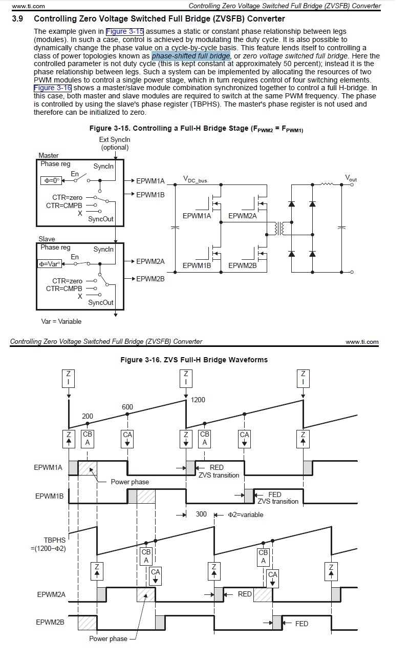
    We require three UCC for open loop commutation in Full-H bridge switching (Fig 3-16) by leveraging rapid duty cycle changes boosting / rolling inductive currents in motors stator.  

    That phase shift via UCC is very little on startup (<20ns) and attempting to adjust the pulse width wider for producing inductor power in H-Bridge mode randomly causes high voltage and (pulse inversions), not overshoot.


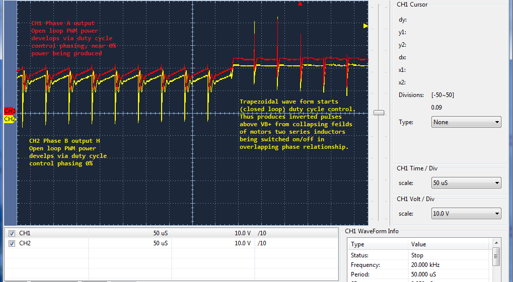
  • Below is zoomed capture of two motor phases A/B showing overlapping from two UCC working together as a full H bridge then switching into 3 phase commutation (closed loop). Notice there is no phase shift occurring as the duty cycle is being rapidly updated in both phases even as changes are being input to HI/LI inputs. It appears the UCC HI/LI delay matching is stripping off the required phase shift from the rapid duty cycle changes. It is true each MCU PWM generator produces two center aligned overlapping signals (A/B) each with a different duty cycle. The three PWM generators are synchronized and produce the same two signal pairs previously described.  

  • Seems this issues started several weeks ago by reversing HI/LI UCC #3 in software pin map, correcting that all seemed ok. Motor was able to start in open loop H bridge commutation and run in closed loop half bridge mode. Replaced UCC #3 (obviously defective) was also causing Cboot charge issues other two UCC. Previous posts were LO not able to fully charge (pull down) floating Cboot to ground in last two UCC, though 1st UCC could so it should still be ok but replaced it anyway.

    First replaced UCC gate drivers #1 & #2 noticing Cboot discharge rising slope returned to UCC #2 but still no phase shift as above capture shows. Replaced #3 and PWM is again producing required phase shift between any two phases.

  • Who would ever suspect not one but Two gate drivers were damaged by reversing HI/LI for short time to one gate driver? Reversal of HI/LI is a common occurrence in past has never damaged the HO/LO outputs of other vendors gate drivers. Oddly the MCU driven PWM is only producing 400-500mA and peaks of 2A during motor run.  
     
    Perhaps HO/LO were subjected above IGPK+/- (4amps <10us) pulsed near 100% duty cycle and H bridge power mode pushed the envelope in two UCC gate drivers?

  • Hi Don,

    Perhaps your team member could comment below how reversing HI/LI on one gate driver for a short period of time could result in this mayhem. Especially as the startup current in duty cycle control was kept very low. After changing HI/LI to one gate driver there was high voltage being produced in the phases and start up DC current surge would often POR the MCU. Oddly there is no real difference in the DMM diode drops between UCC HO/LO outputs yet LO of one UCC has slightly higher ohmic reading than the other two drivers.

    This is a learning opportunity for everyone to gain knowledge of posting ill fated misdiagnosed mayhem and perceived condition of HS jumping to HO during Cboot discharging. That seemingly was caused by the LO output somehow, even internally leaking voltage keeping Cboot partially charged as it was being discharged to ground via 20Khz LO on times.
  • Hi BP101,

    I don't see how swapping LI/HI could damage the part itself. The high-side has UVLO on it that keeps it off until Cboot comes up.
  • Hi Don,

    Perhaps you are correct as we did also connect inverter to a larger motor 12.5Khz and it would not start, only POR's MCU several time. That may have been what caused UCC to fail as being described below.

    Same failure of UCC occurred again, after attempting several times to get large motor to startup at 40Khz (25us) PWM frequency, as smaller motor could easily do. Our inverter FETS have similar QG of IGBT module used TIDA-00778, so we used very same GTRon/off  resistance values shown in schematic. UCC HO/LO drives had GTRon = 6R,  GTRoff = 12R . Perhaps the TIDA engineer miscalculated total QG of the IGBT module relative to UCC to produce IGPK +/- 4amp <10us pulse shorted to ground. Otherwise it seems an anomalous condition can occur relative to the EN pin which destroys the gate drivers HS pin internally when even half QG is expected on HO drive.

    PWM pulses HO/LO in first 250us produce (0-5us leading into 20us pulse widths) and MCU quickly shut down EN pin as over voltage was occurring on DC bus PWM 40Khz (25us) pulse widths. We then doubled GTRon/off resistance values and reduced HO output drive by half. We noticed the charge pump seems to over drive HO during LOW voltage testing UCC @24vdc thus producing high voltage peaks in the DC inverter connected phases.

    It would seem datasheets  IGPK +/- 4 amp <10us pulsed to ground specification is questionable under low voltage drive conditions of HS, when EN is suddenly disabling HO by MCU control. This seems to destroy UCC HO drive yet there is no specific ohmic or diode drop difference (HS-HB-HO) detected on a failed UCC. Once the IC has failed internally ? it then causes (excessively) high voltage to be produced on the DC bus from HS float jumping up to B+ rail. We were seeing +180v produced from +24vdc power supply with large magnet motor, such large potential spikes quickly POR the MCU after gate driver failure occurs. The total QG formula used to calculate HO/LO drive seems to miss the target by a mile under the conditions listed here.

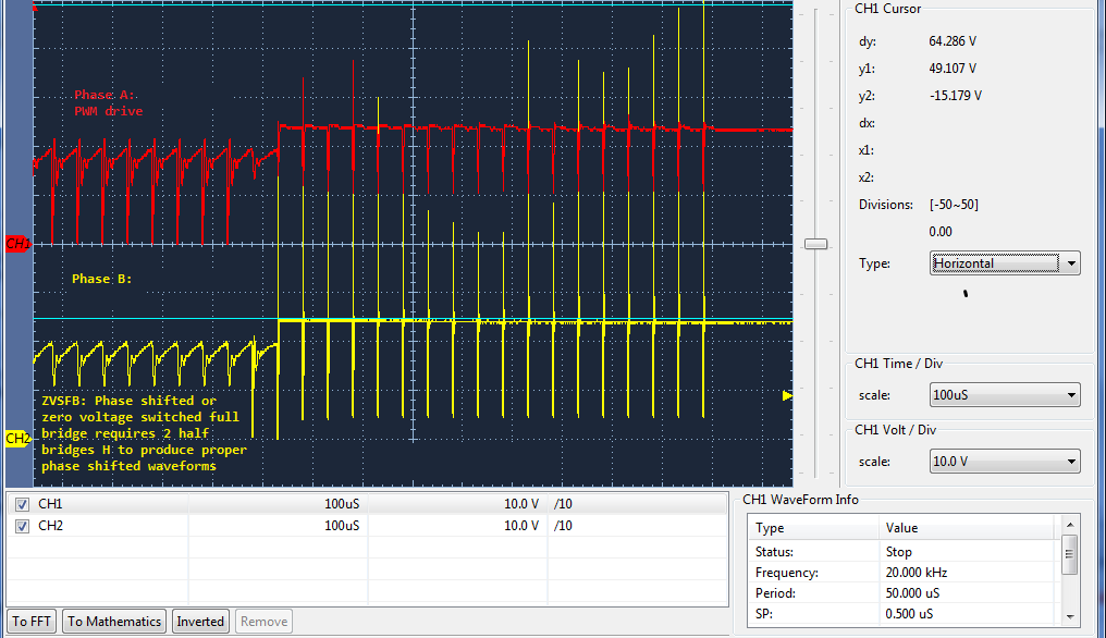
    Failed UCC capture: HS pin will not pull down during Cboot charging via LO driving NFET. HS appears to jump up to HO after Cboot actually being kept in a charged state from HS leakage. So LO can not pull down a floating Cboot in this capture below, resulting in high voltage inverted pulses being produce by HO driving NFET's.

  • CH2 phase B second capture is a defective UCC. Notice horizontal lines between pulses seem to indicate Cboot is not being discharged by LO.
  • Hi BP101,

    Thanks for the clarification. Do you mean to say Cboot is not being CHARGED by LO?
  • Don Dapkus said:
    Do you mean to say Cboot is not being CHARGED by LO?

    Right it is not being fully charged and can not seemingly since HS is leaking current onto the charge/discharge path. That's why the left side of signal is not going all the way to ground a millisecond or so after LO is made low and the HO side NFET peaks are inverted and produce very high voltage bus voltage.

    The condition was so difficult to trouble shoot since HO is mostly functional accept for the leakage current resulting on HS and it interfering with Cboot. Now have 4 failed UCC producing the same HS leakage condition. So far with double the gate drive resistance (HO/LO) leakage has not occurred again but issue should not have occurred at all it seems, especially with 24vdc testing??? 

  • Hi BP101,

    I wonder if the issue is negative voltage spikes? HO and LO have a -2V rating, while HS has a -8V rating. I wonder if you have very small negative spikes that are damaging the ICs?

    these spikes are sometimes difficult to measure - we like to use a "pigtail" like shown in Figure 2 of this blog: e2e.ti.com/.../how-you-measure-your-ripple-can-make-you-or-break-you
  • Don Dapkus said:
    I wonder if the issue is negative voltage spikes? HO and LO have a -2V rating, while HS has a -8V rating

    If that were true would not phantom (di/dt) spikes still occur no matter the gate driver resistance values being doubled? It is more likely the formula TIDA-00778 engineer used for IGBT module QG determination is not specifically relative to HO/LO IGBP(-/+) 4 amps even though he captures (+/-) 2 amps peaks @2KW drive. IGBT modules are by no means quitter than NFET and Infineon OptiMOS-FD reduces diode Trr (di/dt) Qrr roughly 20% over typical industry NFETS. FD technology NFETS run 10 degrees cooler, much like GAN modules reduce body diode Qrr. OptiMOS-FD technology reduces (di/dt) reverse recovery spike jotting below ground, reduced Qrr seems to rule that (-8v) spike idea a mute point.

    Odd idea a negative spike takes out HS input @24vdc when rated -8vdc. Figures 52/53 graph captures indicate even more negative tolerable down -80vdc @100ns.  Perhaps questionable benchmark results being put into the datasheet relative to HB/HS negative tolerance? And our UCC HB bias roughly 13.6vdc, lower than 15v shown in figure 53 should produce even less negative spike. Even at 1us figure 53 indicates -15vdc and slowly slopes up to -8v at some unknown graph time.

    OptiMOS-FD disclosure:

    /cfs-file/__key/communityserver-discussions-components-files/196/1830.Infineon_2D00_Power_5F00_MOSFET_5F00_OptiMOS_5F00_FD_5F00_200V_2D00_250V_5F00_hard_5F00_diode_5F00_commutation_2D00_AN_2D00_v01_5F00_00_2D00_EN.pdf

  • Hi bp101,

    Maybe not HS, but maybe the inputs or Ho or LO?

    And, yes, doubling the gate resistance will slow down the dv/dt on HS which helps reduce voltage spikes induced in the stray inductance in the power loop. As I mentioned above, these spikes are sometimes hard to catch. Using a standard alligator ground clip may hide them from view. That’s why we use the pigtail method.
  • Hi Don,

    A curve tracer might reveal what was being damaged but we suspect HS input (lower Totempole FET) is not holding up under HO load, IGPK-/+ amp <10us pulse. Yet going from scope captures observation it appears HS then leaks current via HB since LO can not pull HS or Cboot to ground after a failure occurs. Seemingly going from past experience with other vendors gate drivers a negative spike/s should not destroy HS or HO FET structures @24VDC supply. Perhaps that misconception under these small load conditions has lead you to believe such is even possible. One thing negative spikes may do is turn on HO drive with out HI directive, cause LO side shoot through which did not occur in the last UCC gate driver failure we directly witnessed happen. 

    The only thing that changed to stop UCC failures was to increase gate resistance values several times greater than NFET total QG value. That alone makes the IGPK(+/-) 4 amp <10us pulse short to ground and di/dt graph (-80v Figure 53) both misleading facts. Perhaps IGPK+/- 2 amps would be more conservative in light of unexpected failures others are sure to report in this forum.

    TIDA-00778 shows a +/-2amp gate drive (sine wave pulse) current on HO/LO, that does that imply a (square wave pulse) holds true too under similar conditions. Our PCB has forced air flow (139 CFM) and small ground plane under each UCC foot print, helps pull SOIC package thermal heat out of silicon die extending power handling characteristics. Seemingly the only reason both HS/HO outputs are not being stressed is (DSP sine wave) was being generated on both HO/LO outputs.  Likewise a square wave has faster rise/fall times than DSP sine wave has considerable roll off (top/bottom) of wave form compared to a basic square wave pulse.  

    Perhaps TI lab analysis did only sine wave pulse testing of IGPK +/- 4 amp <10us short to ground, Output Block conditions? 


  • Hi BP101,

    As you stated, the output current is limited by the internal gate resistance of the switching element (FET, IGBT, etc) as well as the gate resistor.

    We recently published a Tech Note on how to calculate the gate resistor:

    www.ti.com/.../slla385.pdf
  • Hi Don,

    Don't know who authored PDF but quote below taken from (Fig.3) is not exactly correct. NFET body diode Trr requires time for total Qrr recovery and higher values of Rg create more recover time and reduce dv/dt turn on ring (overshoot), di/dt spiking below ground. The Infineon OptiMOS-FD (fast diode) NFET should not pose such Trr/Qrr issues and out perform typical IGBT modules using similar Rg values.

    TIDA-00778 engineer added 2200pf caps across HO/HS increasing IGBT modules CGs, producing Rg slushing (edge roll off). Perhaps high frequency HO roll off slows gate turn on, allows for slower (Trr) and masks lower value Rg chosen for HO commutation. NFET Qg or inductive resistance is not the only things to calculate in any formula that determines proper Rg values, when Trr is being left out of the Rg equation.

    That said the UCC gate driver HO output design seems to over drive certain NFET's in the miller effect area. Seemingly Cboot (value) RC time constant calculations may be some cause with certain NFETS such as OptiMOS-FD. May not require hard HO commutation at all points of inductive loading to reduce body diode effecting (Trr) ringing. It would seem BLDC motors inductance Q/R changes as the rotor load adjusts to a steady state or PWM duty cycle. That is one reason HO driven NFET overshoot diminishes from fewer avalanche (Ias) events when HO rising edge is slowed relative to LO. So there is more to the HO story than what the PDF is relating and leaving out NFET Trr in the calculation seems a bad example.

    quote: "Also, higher resistor values will overdamp the oscillation and extend the switching times without offering much benefit for the gate drive design."