This thread has been locked.

If you have a related question, please click the "Ask a related question" button in the top right corner. The newly created question will be automatically linked to this question.

UCC27714: HO & LO ghosted ringing

Guru 54057 points
Part Number: UCC27714
Other Parts Discussed in Thread: TIDA-00778, , TIDA-00909

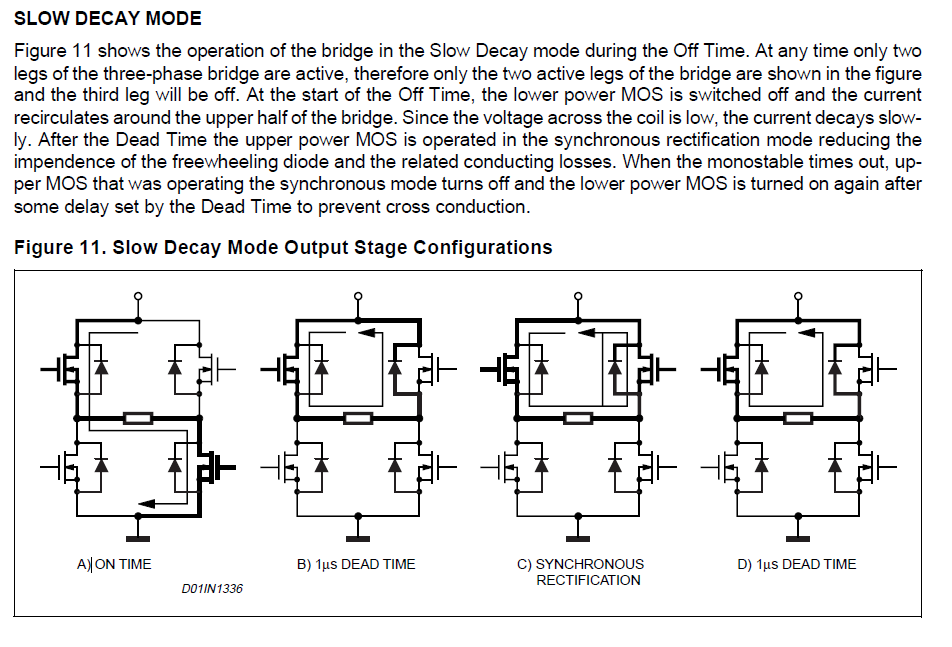
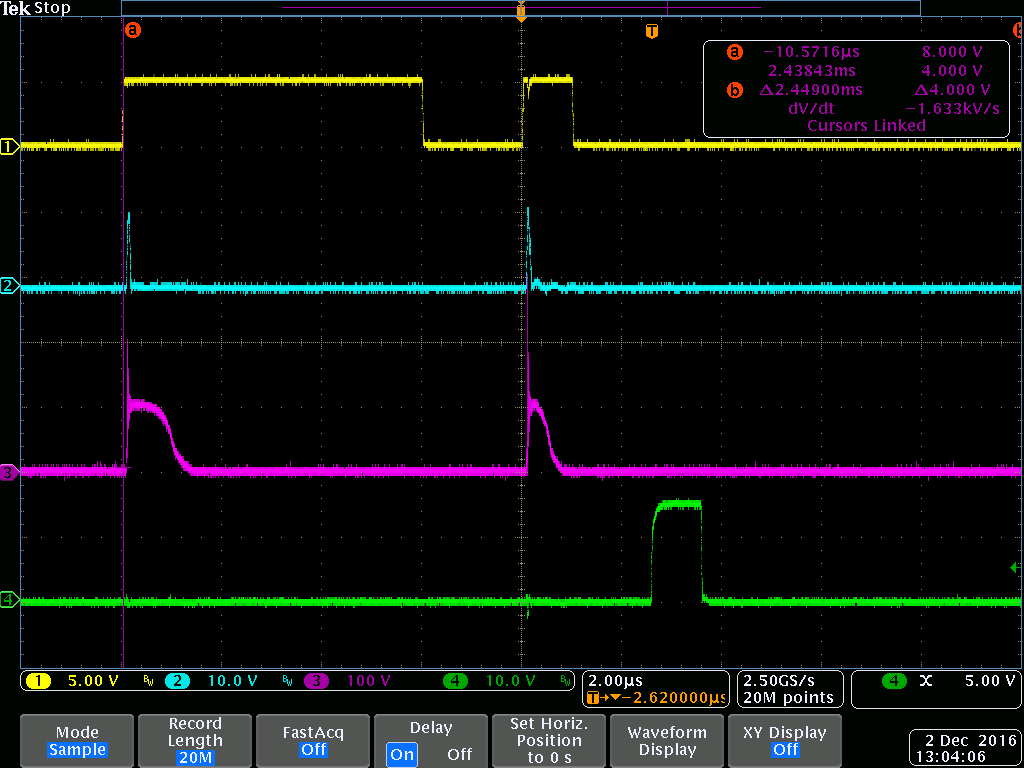
We capture certain position of LO ring ghost or follow HO ring and or undershoot may be HI/LI driven cause? We notice 140ns 1/2 bridge dead band delay make HO incorrectly produce 140ns positive pulse when it should be delay time only. If we make 100ns delay the HO pulses diminish into a minimal sine wave when HO transitions from high to low but not entirely in every case. The Gton=530ma and GtOff=1.5amp yet we have never heard of Toff switch node ringing or odd HO/LO ghosting captures show below. Especially when inverted LO is producing short HO pulses between the main trapezoidal waveforms. Only HI is inverted and derived from LI during delay periods but only for a previous high to low transition of HO in any current output period does a delay occur.   

Perhaps UCC shorter Tfall 30ns, 125ns propagation delay and faster NFET Toff 24ns delay, 8ns fall time allow even shorter dead band period than 100ns? How minimal can 1/2 bridge dead time delay be made when NFET Trr is 144ns Nom to 288ns Max? Can some HI/LI dead band generator phasing be causing random pulses in the HO period but only when LO high to low? 

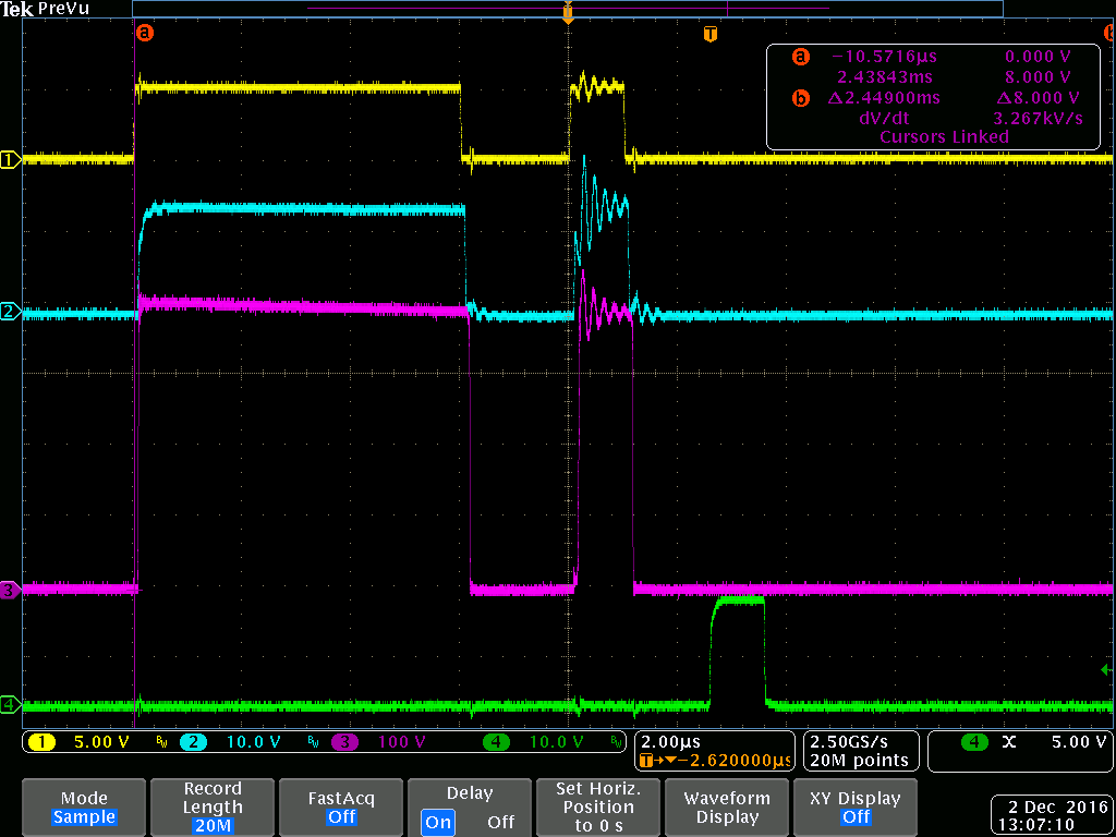
Updated capture below after bravely setting dead band generator 60-80ns. Most documents suggest dead band delay be set 1.5 - 2 times the minimum pulse width. So 0.8us (800ns) minimum pulse width makes dead band delay 1.2us but not 80ns. Perhaps the PWM generators minimum pulse width is set to high in software algorithm! 

  • Hi BP101,

    For your scope shot showing "LO pulses make HO ghost pulses" how are you measuring HO? Are you using a differential probe? If not, where is the ground for the oscilloscope probe?

    And, is LO really high for 3.5 ms? That seems like a long time.
  • Hi Don,

    I think your missing the bigger point to determine why HO follow LO undershoot. In that aspect does it really matter HO ground is common. The PWM frequency 12.5Khz(80us) period, LO pulses are near 100% duty (79.85us) indicating high side NFET in slow decay. Slow decay artifact can be seen as LO pulse reach near NFET Ton 4.6v threshold, LO side NFET is mostly saturated, HO is switched for speed control duty cycles. Welcome to slow decay mode, produces power from inductive recirculating current in HO side NFETS.

    The question is how short can dead delay be safely made given added delay of gate driver and NFET Toff fall/delay time. Do we subtract gate driver added delays or add it to dead band period? When we add gate driver delays to NFET Toff fall time/delay, gate driver produces artifacts of (excessive) undershoot condition. Undershoot drives DC Bus Voltage upward as a result, shorter dead delay trimmed 18vdc off inductive voltage rise and reduced most of HO undershoot but not all.  

    Slow Decay:

  • Perhaps there is a hidden timing problem between HI/LI as partially proven by reducing dead band delay period, HO undershoot is significantly reduced!

    The capture of LO you question 3.5ms (yellow square) is 60 degrees PWM window of many 80us periods where software controlled dead band delay occurs prior to each new/next period. Those HO undershoot pulses -6v or more at times are not UCC killers but should not be produced at all in slow decay. Only fast decay produces pulses from ground up to HO rail in that same (yellow square) area.

    The question is how to stop remaining HO undershoot as the LO side is not for this 1/2 bridge HO inductor leg (captured) but another gate drivers HO leg. LO was scope trigger source most captures above. It seems the HO undershoot pulses are occurring from UCC internal creepage or MCU HI/LI timing is not sharp enough for UCC. The VDD pin has 10uf to digital ground trace and common pin 1uf to analog ground plane provided by low side NFET from VIA to analog ground plane under side of PCB. Past other vendors gate driver we tested similar filter (HI/LI 100R/200pf) produced excessive rising edge roll off. UCC rising edge seems ok with 51R1/200pf but have you noticed any HI roll off cause any issues with HO drive relative LO?

  • Hi BP101,

    My first thought when you say it gets better with decreasing dead-time is Irr current goofing things up.

    You've mentioned competitor parts several times in your post. I might suggest you try one of their devices in your circuit to see if this issue is our device, PCB layout, firmware, etc, etc. You seem to be really struggling with your design, and I can't figure out why...
  • Hi Don,

    Other vendors gate driver also had a little of same undershoot along ground. So far 80ns dead time seems to work for 24v but a single HO output was quickly compromised initial 80vdc testing. First few pulses and one HO output was compromised @526ma source, 1.085A sink in an 80us period of fast decay starting with 0% duty cycles rapidly increasing them in 18700us commutation hold period.

    It would seem the claim of UCC to consistently produce +/-IGPK 4 amps is in serious doubt relative to HI/LI duty cycle controls. Oddly HO driven overshoot voltage occurs on NFET drain. Might this ringing be due to HO overdriving the high side NFET, seemingly it is not under full MCU control. Perhaps Cboot must be sized below 1uf or the Totem pole bias is excessive in driving HO?

    Forum engineer Derek did not fully answer past post how UCC enhanced Miller plateau is relative to Cboot value changes from other vendors gate drivers. The reasons given for TIDA-00778 selecting 1uf Cboot value perhaps do not produce good results when the wave form is other then DSP driven sinusoidal? Should that not be a concern of TI engineering since they enhanced the Miller plateau and HO drive performance? Silicon Labs Cboot calculator suggested 0.12uf capacitor not 1uf as we too past used.

    Why would a NFET QG-89NC and HO GateR 24R/24R cause the HO drive to be compromised? Previously used 60R/10R for QG-91NC with other vendors driver, (+/- IGPK 350ma/650ma, PW < 10us short to ground) up to 190VDC with none of these odd issues now facing.

    That said it would seem the UCC is for some reason over driving HO output when the MCU HI/LI duty cycle is not directing it to do so. That is why we twice had to increase GateR source/sink values, now 24R/24R. Where is the end to how much we must reduce HO drive IGPK so it does not compromise the high side Totem pole? Something is not adding up in how calculations of Cboot and Rgate should be made. Likewise TIDA-00778 engineers evaluation of UCC27714 gate driver for an IGBT module having QG-275NC is not a definitive analysis by any means since the UCC datasheet also claims it suitable for NFETS. How did TI lab determine or not that Cboot was not a part of the Miller plateau analysis relative to industry standard gate driver designs? Might there be some major ramifications to disclose in datasheet relative to HO side Totem pole bias currents derived from Cboot values in light of Miller plateau changes?

  • An interesting fact is other gate driver circuit (prototype) did not have 10uf on VDD pin or 5R1 bias to +15V supply to protect gate driver from UVLO. It was direct coupled +15 VCC rail with one 22uf cap and 100nf to ground each gate drivers VCC pin. None of this exotic UVLO bias filter tank or a COM pin bypass cap the UCC requires.

    Checking with scope for 10Mhz ring source in +15 VDD supply notice the same millivolt ringing signature as viewed on NFET sources. Could the 10Mhz ringing be self inflicted by the UCC's internal UVLO circuit relative to capacitors selected for VDD/COM pins?

  • Hi BP101,

    I suppose it could, or it could be ringing due to parasitic inductance in the loop. You might want to try placing a cap with low impedance at 10MHz to try and squash the ringing you are seeing at that frequency.

    Reminding you of a couple things. First, the effective capacitance goes down with dc voltage applied across it, so make sure you have enough capacitance when running with dc voltage across it:

    When I say for 10 MHz - choose the lowest impedance point to be at 10 MHz. You can use several caps (of different values, and hence different minimum impedance frequencies) to get a low impedance across a wider range of frequencies:

  • Hi Don,

    Having tried different cap values for VDD bypass @Dboot anode had no effect what so ever to calm voltage spikes that proceed the 10Mhz ringing cycles. The ringing is ok but the spike has to go!

    It seems the HO ringing frequency (10Mhz) is being amplified by NFET and body diode (Trr) has not enough time to snub inductive EMF to ground during LO (saturated) off times.  

    Part of the problem is trying to identify what is causing HO to oscillate where the LO side NFET body diode fails to snub CCEMF. Perhaps LO blocks current to ground, quickly switching on again during HO trr. That may have something to do with LO side NFET being 90% saturated and HO side NFET slow current decay (randomly) driving voltage spikes onto B+.

    So UCC faster HI/LI rise times coupled with 90ns propagation delay seem to enhance an already bad attribute of slow current decay.

  • BTW:
    Yesterday changed HO Rgate from 50 to 75 ohms. That smoothed out the first low dip in ringing signature and reduced the peak voltage spikes. So it seems HO (randomly) over drives the NFET gate thus exacerbates (amplifies) inductive current oscillations in the process. The Totem pole drive to HO output is at times acting like an amplifier producing uncontrolled current gain in the NFET gate.

    Oddly the ringing frequency often surpasses 12.5Mhz up to 13.3Mhz is 1000 times that of the PWM 12.5Khz frequency.
  • Hi BP101,

    Any time there's a fast edge in the switching circuit, there's a possibility for this switching edge to couple into other circuit elements through the parasitic components. These fast edges in switching converters typically couple through the parasitic capacitances of the MOSFET and back into the gate driver, and there's usually a small inductive component on account of the MOSFET leads and the trace characteristics which cause it to oscillate at a high frequency. It seems you have two fast edges to consider: switch node transitions from a conducting MOSFET channel to a conducting MOSFET body diode, and switch node transitions from a conducting MOSFET body diode back to a conducting MOSFET (A->B and D->A in your diagram). The first transition is largely a function of the turn-off speed of LO and the inductive current driving the parasitic capacitance of the MOSFET, so by increasing the gate resistor it's possible that the switch node transition is being slowed and the high frequency content of the signal is attenuated, reducing the observed effect on the gate driver. The second is a function of how much current remains in the body diode when the other conducting MOSFET is reactivated, and that reverse recovery spike can be very nasty and sometimes causes switch node slewing much faster than intended thanks to the very high reverse recovery current that can develop. Aside from using a discrete diode with little or no reverse recovery in parallel, this effect is hard to deal with, but can be minimized by reducing the body diode current to a minimum before switching the other MOSFET on, placing a better diode in parallel with the MOSFET drain-source, or using a switch with a copackaged or optimized rectifier.

    Occasionally, I have found a ferrite bead with a high impedance at the ringing frequency can smother that coupled ringing. Since the gate resistor values are relatively large, I think you shouldn't have much trouble putting a 10MHz ferrite on your gate drive lines.

    Regards,
  • Hi Derek,

    Derek Payne said:
    The second is a function of how much current remains in the body diode when the other conducting MOSFET is reactivated, and that reverse recovery spike can be very nasty

    Albeit HO is simply switching on the gate when the voltage spike occurs NFET source, so that is not diode Trr until HO switches off in dead bands well before LO copartner. What we are seeing is the effect of Totem pole oscillating from over driving NFET gate after Miller plateau has been reached, no pause. Agree the HO slew rate is far to fast thus seems to cause random overshoot just above Miller region. So source perhaps develops excessive number of holes ride on HS, seen as magnitude increases in the ringing effect.  

    Perhaps protection 20k resistor across HO/HS pins fails to clamp faster source depletion holes entering HS pin, back out HO as aggravate inductive ringing spikes. Voltage magnitude grows uncontrolled in first pulse relative to charge pump floating voltage conditions at that time. The kind of info lacking in datasheets or other PDF documents, thus we need help to determine how UCC over other vendors gate driver is randomly increasing gate drive current (after Miller) as the switch peak is being reached only during HO turn on state. Hard to imagine 16.5v zener diodes placed across HO/HS may aggravate inductive ringing, mostly HO rings not so much at all LO. Again some ring is ok but the voltage peaks HO produce in NFET source are far to high for safe operation when approaching BVRdss.  That never occurred in slower gate drivers coupled with even slower Trr.

    BTW above link below posted PDF, Infineon OPTIMOS-FD (fast diode) has 20% faster Trr than our previous HEXFET slower Trr,  was producing less source ring magnitude with much slower gate driver. We never saw turn on peaks exceed +10v of drain voltage with a local DC bus voltage cap (470uf) and now two 680uf parallel 1360uf low ESR rated 1.9 amp ripple voltage. So surprised 24vdc HO randomly was producing over 90v lastly up to 50v switch turn on peaks (HO/75R) in the first ring pulse. Ideally if the UCC HO/LO slew rates are to fast we better slow down HI/LI slew rates? Documents suggest to increase HI/LI slew rates, perhaps faster is not always better?

    How does HB/HS relate to HO in current drive aspect when NFET source holes enter HS relative to chosen external resistance values?

  • Other forum post shows same issue but in a different discussion how IAS will become a problem with NFET BVRdss being exceeded via aggravate ringing pulse. Had originally thought spikes were result of IAS event but the top of spike is not flat according to later Infineon PDF, flat top signature BVRdss left out of an earlier PDF technical brief. This pulse captured below will lead to single pulse IAS events shown in other post link. We are sourcing 200vdc NFETS and drains are only 24vdc (below) other HEXFETS were ok up to 165vdc via slower gate drivers and a much rougher 3 phase PCB inverter.
     
    e2e.ti.com/.../699252

    Recent capture HO, 60- 80ns dead band time reduced phantom pulsing, likely part of PWM generators minimum pulse width showing face.


  • BP101,

    Am I correct in understanding that you are testing with a 24V bus, and you are driving 200V FETs? Most MOSFETs are designed to be operated between 50% to 70% of their rated voltage if used for switching, and there will be significant ringing at lower voltages due to the changing parasitic capacitance of the MOSFET across voltage. See the graphic below. When switching in the red region, the change in capacitance will cause substantial ringing; when switching in the blue region, the parasitic capacitance has settled to a rough final value, and the ringing will be substantially reduced.

    We see this effect all the time when using UCC27714 to drive 600V MOSFETs with system bus voltages of around 100V-150V. Consider the following double pulse test, where CH1 is HI, CH2 is HO, CH3 is HS, and CH4 is LO. The inductive load is tied from HS to GND. The bus voltage is set to 100V. Note that the dv/dt of the transient is over 150V/ns, and operating so far outside of the driver's absolute maximum ratings is causing missing pulses on the driver output:

    There is 300V of switch node ringing. Below is the exact same circuit at 400V bus voltage:

    There is about 50V of switch node ringing, and it is reverse-recovery related. The initial pulse, with no reverse recovery, has barely 20V of ringing.

    How does your system behave when your chosen MOSFET is switched at its target bus voltage?

    Regards,

  • Hi Derek,

    Thanks for investigating this issue and taking the time to understand what is going on in this case issue.
    Sadly the problem gets worse with higher VDSS well above 24v, the inductor Q should drop as voltage is increased. Our case the load into HS is not tied to ground rather HS of copartner 1/2 bridge. Even though LO is high in that same 1/2 bridge, HS is exposed but clamped off to HO. Yet Cboot is charged during this same time according to Infineon documents.

    Please lets end this thread getting long as 80v VDSS typically produces in excess of 138-142 volt peaks posted in other thread. Again it's not the ringing being directly the problem it is the result that occurs in the secondary pulse amplitudes exceeding well beyond VDSS. That alone becomes a major problem as monitored bus voltage is easily tripped unless set well above a safety level, 10-20v above VDSS. So at 165VDSS we would have to set the safety monitor above NFET's BVRdss 200v. The high peaks also lead to MCU issues in the ADC samples being compromised from FB. That will never fly....

    As explained we past used other 600v gate drivers that did not produce uncontrolled voltage peaks, even at 24vdc. The UCC HO output is not limiting drive current by only a resistor, may be part of the problem, perhaps not entirely. For example we tested the same inverter up to 192VDSS with 250VBRdss NFETS without tripping the safety monitor set 5v above. Course inductors cause VDSS to quickly fall off but the point is the ringing peaks never exceed much above VDSS.
  • BTW:

    Derek Payne said:
    There is about 50V of switch node ringing, and it is reverse-recovery related. The initial pulse, with no reverse recovery, has barely 20V of ringing

    Notice our secondary pulse is not Trr recovery related, it is the next 80us HO on time and diode recovery is occurring relative to HS near ground not above HS as shown in your captures.

    In my opinion that ringing in our capture shown on the secondary pulse is not Trr recovery as the gate or DS are never switched off, negating Trr recovery in that time frame. How could HO NFET body diode enter reverse recovery when DS are near VDSS thus making it reverse biased in our capture. The secondary pulse in our capture is result of inductive current flow via DS causing said ring. 

  • Hi Derek,

    Derek Payne said:
    Note that the dv/dt of the transient is over 150V/ns, and operating so far outside of the driver's absolute maximum ratings is causing missing pulses on the driver output:

    And note we do not have this issue as the entire rise of VDS is less then a few nanoseconds.  

    Derek Payne said:
    There is about 50V of switch node ringing, and it is reverse-recovery related

    Albeit Trr/Qrr recovery occurs below VDS shown in your/our captures during gate turn off time.

    What it seems we are seeing and trying to reduce (VDS peak) reacting to inductive inrush current, especially noticed on the second pulse, every other pulse after. Hence the rapid rise of VDS into inductors point of saturation is perhaps to accelerated via HO thus causes current ring in the inductor, e.g. current leads the voltage in an inductor. That inductive voltage ringing is contrary to the idea voltage is the electrical presser behind current, scope sees voltage as an artifact of the surge current. That seems to explain why the same value gate resistance used with slower gate drivers has more effect to slow inrush current into the inductors. Perhaps a softer start cycle above Miller could reduce inrush current into the inductor and increase switching efficiency. Hence the other thread was believed more prudent to that idea.

    Attached is a excellent PDF from Infineon, OPTIMOS-FD NFETS we are using have improved Trr/Qrr over typical NFETS.

    /cfs-file/__key/communityserver-discussions-components-files/196/0218.0820.Infineon_2D00_Power_5F00_MOSFET_5F00_OptiMOS_5F00_FD_5F00_200V_2D00_250V_5F00_hard_5F00_diode_5F00_commutation_2D00_AN_2D00_v01_5F00_00_2D00_EN.pdf

  • Hi Derek,

    Derek Payne said:
    There is 300V of switch node ringing. Below is the exact same circuit at 400V bus voltage:

    I have also seen inductive ringing lumped into diode recovery in some earlier DUT testing. The later PDF attached above has better detail relative to diode Qrr. Besides how can the NFET be recovering when it has just reached peak VDS.? Seemingly free wheel body diode Qrr occurs mostly after NFET turn off during dead band so HV inductive kickback does not destroy the junction, snubs it. 

    Perhaps why HO softer current drive reduces high VDS peaks after higher gate resistance, ringing softens. That slows down HO totem pole current into the gate region so the DS slews a bit slower in the process, after Miller 2. One fear was not knowing how high resistance might effect the NFET threshold relative to data collected from other gate drivers with slower slew rate and lower current drive. The wires to our motor stator are a bit long (3.5'), likely not helping ringing yet true AC induction motor does not seem to have wire length issues. So find it odd that synthesized AC current (Trapezoidal wave) is directly responsible for the inductive ringing as GAN integrated driver module rings just as bad with sine wave PWM, TIDA-00909.