This thread has been locked.

If you have a related question, please click the "Ask a related question" button in the top right corner. The newly created question will be automatically linked to this question.

UCC27714: How to slow HO rise time for NFET soft start cycles

Guru 54057 points
Part Number: UCC27714
Other Parts Discussed in Thread: TIDA-00778,

How can we without further increasing gate turn on/off resistance slow down HO rise to miller plateau to reduce NFET surging IAS events?

Can Cboot value directly impact the NFET QD-nc in such a way HO is to fast thus driving BVDSS excessively high? Perhaps the HO Totem pole enhancement (PChannel assist) can impact high side NFETS in a bad way too. Noticing HO driven DS rise time <50ns to Miller plateau and <100ns in first pulse often rising well over BVDSS source voltage. Example; NFET with 24v BVDSS is randomly producing well over 45v IAS peaks, not a safe condition. That NFET QG=89nc yet 24R/24R ohm gate drive can compromise HO output with higher BVDSS source 80volts recently tested.     

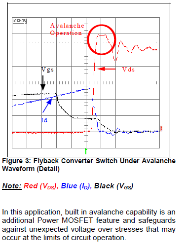
Might Rboot/Cboot RC time constant values chosen for typical industry gate drivers, with UCC effect NFET in driving excessive pre-mature IAS events? Otherwise what is the purpose for +/-IGPK 4 amp <10us PW if the HO output is easily compromised with typical Rboot/Cboot RC time constant often chosen for lesser speed gate drivers? The idea in my mind is faster UCC HO slew rate ability needs to be regulated for soft start boot charge cycles, not simply push the Miller plateau and drive IAS events in the process. The ringing often occurring after the Miller plateau according to Infineon is an IAS event not necessarily caused by stray parasitic.


  • I do realize Figure 3 shows a gate turn off event casing many IAS events. Yet the very same ringing signature is present at peak gate turn on time. Logically HO driven NFET turn on ringing events are thus (partial) IAS events protecting the DS from destruction due to gate region being overly saturated.

  • Hi BP101,

    I was wondering where you pulled that picture from, and after a quick Google search, I found my old colleague had written it... That made me smile! Small world.

    Anyway, in that section, I believe they are talking about unclamped inductive loads. If I understand your circuit, the high-side FET's diode will clamp the output to your high voltage rail + its diode drop when the low-side FET switched off (during the dead-time, until the high-side FET is turned on, at which point the channel will carry the current instead of the body diode).

    I think the best way to tune your switching times is to use a gate resistor network. The resistor in series with the bootstrap diode is used to limit the peak current thru the diode so it isn't damaged (at start-up, it is basically short-circuited until some charge builds up on the bootstrap capacitor). It is out of the circuit when the high-side FET is being driven as the bootstrap diode is then reverse-biased due to HS flying up to the high-voltage rail. CBOOT should be directly connected across VB and HS to provide a stiff supply for the high-side gate driver.

    This is discussed in this app note: www.ti.com/.../slua618.pdf. See section 5.2.2.3 Bootstrap Switching Action
  • Hi Don,

    Don Dapkus said:
    I believe they are talking about unclamped inductive loads

    Exactly the 3 phase motor circuit does not have a separate snubber other than NFET freewheeling body diodes. Thus providing synchronous rectification protecting each NFET from inductive kickback. The high side NFETS in slow current decay recirculate the inductors current so the body diode has more time to rectify any inductive kickback voltage. 

    Don Dapkus said:
    I think the best way to tune your switching times is to use a gate resistor network.

    Already have a network in place Schottky diode in series with 24R for gate turn off.

    Don Dapkus said:
    It is out of the circuit when the high-side FET is being driven as the bootstrap diode is then reverse-biased due to HS flying up to the high-voltage rai.

    We discovered this week that is not entirely true at least during pre-charge phase it is easy to prove. One phase's LO being turned on can directly impact another phase's half bridge Cboot charge cycle. It happens via the co-partners inductor wire. So Cboot of one 1/2 bridge is being charged by another or Co-partners 1/2 bridge at the beginning of each of it's Boot charge cycles. Infineon mentions this same condition (OPTIMOS-FD) but in the single 1/2 bridge not from a co-partner. We had previously installed an 8.2 ohm series resistor to HS on other vendors gate driver plus Schottky from HS to ground to stop IC latch up (e.g. missing pulses) but noticed previous NFET source voltage spiking reduced by also increasing gate drive resistance to 60 ohms.

    Don Dapkus said:
    The resistor in series with the bootstrap diode is used to limit the peak current thru the diode so it isn't damaged

    We were trusting the faster slew rate of UCC HO drive would correct what now seems to be RC time constant Cboot charge related. As describe above the UCC faster HO slew rate seems to have made HO spiking condition worse. Hence the perceived need for HO softer (slower) rise times seems the only way to counter act inductive spiking.

    Don Dapkus said:
    CBOOT should be directly connected across VB and HS to provide a stiff supply for the high-side gate driver.

    The Cboot diodes / resistors are top side of PCB and enter UC pins 11/13 through VIA's directly below. They are directly biased via 15.4v supply rail into each 3R3 resistors feeding the ultra fast 200v diodes (Trr 14ns). 

    Is it possible for a TI engineer to spend some LAB time to determine how the UCC enhanced HO drive in Miller plateau region may effect typical Cboot RC charge times? Perhaps update the datasheet to include options for what can be done to counter act high inductive ringing during HO turn on events?  Perhaps the Cboot charge pump RC time constant is to slow for NFETs of lower QG (1uf typical) as TIDA-00778 engineer & Derek tried to explain away but may have missed this issue entirely.


  • HI Don,

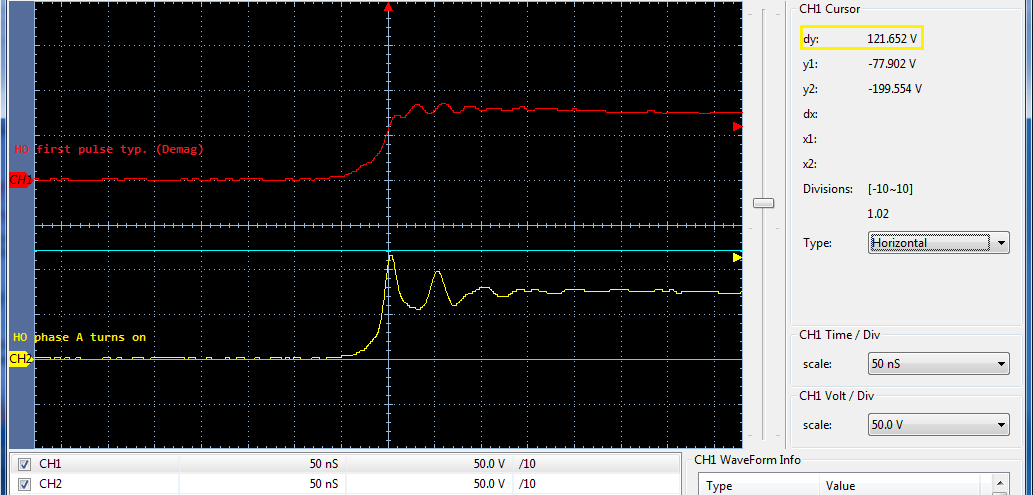
    Doubling gate driver resistance on both LO/HO drives from 24R to Gturn on 51R1, 24R Gturn off and there is no reduction in NFET sources producing 50v peaks. Even though HO Miller plateau went from 50ns up to 100ns the NFET drain to source (HS) between two UCC partners remained 50ns rise or 50v peaks/100ns so (dV/dt) remains <50v/ns. The outcome, NFET source is rising exponentially faster than HO rises to Miller.

    The OPTIMOS-FD NFET has very low (QG-67nc Min/85nc Max), TI Tech note (SLLA385–May 2018) refers IGBT modules and Ls ringing frequency produces much smaller value GateR leading to compromised HS/HO drives. The ringing (10Mhz) of Q=LS/RG formula produce very small values for gate drive resistance thus making the LD of NFET source to drain worse, not better.

    This seems to prove slowing down HO by some 50ns is not the root problem of HO drive. Notice above captures 10Mhz ringing is present on HO turn off events. Perhaps VDD has incorrect bias supply caps, e.g. VDD=10uf, COM= 1uf? Perhaps even very large Cboot value lead to 10Mhz oscillations no matter what the PWM frequency is 12.5Khz to 40Khz, make no difference?

    There is no information in any of these PDF's that specifically answer why 10Mhz is being produced by UCC gate drivers HO/LO outputs.
  • Also seem to believe the inductive load is unclamped not the NFET, since the load does not have a separate snubber. The Infineon PDF mentions a snubber diode/circuit can help to reduce parasitic IAS events in the unclamped inductive load. It seems they use the word unclamped as to mean no devices are installed to mitigate inductive kickback or magnetic CCEMF. 

    We shortened motors inductors (#12 AWG) but did not reduce 10Mhz ringing frequency, that seems to come out of the gate driver HO/LO but may simply be flyback?

    SLUA618–March 2017–Revised SLUP169 – April 2002 mentions the inductors LD reduces under higher drain voltage. In the past HO gate turn on of NFET source spiking/ringing could be reduced @24vdc yet would return at higher voltages (80v-165v). So the 10Mhz oscillation need to be reduced @24vdc which did to some degree reduce spiking via higher gate drive resistance. The HO/LO gate drive loops of our new custom PCB are very short, even shorter than the first custom etched PCB used with other gate drivers. Hard to imagine the PCB is oscillating 10Mhz and is more likely the HO totem pole ringing due to the RC time constant of Cboot overcharging (HB bias) pin?    

  • Hi BP101,

    Please see the other response I just posted on this thread:

    e2e.ti.com/.../2580419
  • Hi Don,

    Yet this thread focuses on the B+ voltage spike that are showing up on HO drive times. Typically the LO side often produce (di/dt) ground spikes during this switching time.

    Hence the confusion on why UCC faster switching times coupled with faster OPTIMOS-FD is causing B+ voltage spikes. Typically HO side current gain (spikes) are directed to ground via LO side NFET body diode. The FD Trr is even faster than the NFETS we previously tested with on a basic PCB. Yes there was some inductive ringing but the B+ spikes were very low, under 10v compared to the 40v spikes we now see.

    Alternatively HO driven NFET current gain can enter B+ via (regulated) control of gate region. There are random times HO fails to control B+ current gain during HO totem poles 10Mhz ringing cycles. Ideally less ring is more in this scenario and past has produced fair tradeoffs with increased Rgate values.
  • The UCC27714 being very fast it is not naturally regulating HO drive current in gate switching. One finding is the NFET requires unusually large value gate turn on resistor (125-150 ohms) jut to slow inductive inrush current surging through the NFET DS junction. The unregulated HO Totem pole drive current is causing very high VDS peaks in low QG NFET. There is some kind of trade off that requires larger gate drive resistors than some would ever consider like, in class specific conditions.

    Certain DRV series gate drivers have the ability to produce soft start gate turn on PWM cycles. One might deduce that would allow smaller value gate drive resistors on HO output without compromising the gate driver in the process. Even when the HO drive current and pulse width are kept below (+/- IGPK 4amps <10us) short to ground the driver can be easily compromised by sudden inrush current caused by rapid HO drive characteristics in NFET switching.
  • Hi BP101,

    Thanks for letting us know!
  • Hi Don,

    Perhaps TI has fallen short in fully documenting the effects of the new HO drive structure as it relates to NFETS. Was hoping for backup from TI LAB at some point to investigate why the faster rise to Miller seemingly causes excessive VDS peaks from low QG NFET's. That is relative to slower gate drivers requiring lower value gate resistors to remedy similar condition.

    Would be nice if HS pin could sniff the inductive load current demand and adjust HO current accordingly, perhaps removing the need for any gate resistor at all. We do that in ADC current loop of MCU, adjust PWM duty cycle from feed back monitor. Seemingly loop is not fast enough to remedy HO 50ns rising edge slope.
  • Even the Delfino TMS320-F28037xD with a 1us FCL current loop may not adjust duty cycle fast enough to control the rise time of HO after Miller 2. Would be interesting to test our DC inverter with that MCU to see if any difference occurs in the gate driver loop.