This thread has been locked.

If you have a related question, please click the "Ask a related question" button in the top right corner. The newly created question will be automatically linked to this question.

TPS65105: Not getting proper voltages at output

Part Number: TPS65105
Other Parts Discussed in Thread: TPS65101

Hello,

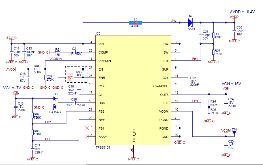
I'm using TPS65105 in my circuit of display driver. I need different voltages for VGH, VGL, AVDD, DVDD, VCOM. Attached is the schematic of TPS65105.

I'm getting AVDD =3.3V and all other outputs 0V.

I have referred below thread for solution

https://e2e.ti.com/support/power_management/lcd_oled_bias/f/954/t/283372

As mentioned their I already have higher capacitor. What could be probable issues?

  • Hello Kushal Shah,

    Did you check the startup to see if the device starts up at all?
    Checking your schematic I understand that you don't want to use the linear regulator. If this is correct, the BASE pin must be connected to VIN and ENR to GND.

    Best regards,
    Diaara
  • Hello Diaara,

    Yes. Device is getting started but protection mode kicks in. Attached is the snapshot of scope measured at VGL.

    .

    Regards,

    Kushal Shah

  • Hello Kushal Shah,

    Please try to find out which of the outputs is not able to start. Please measure all outputs and zoom in enough, that the startup ramp can be observed.

    BTW, I expect that the positive charge pump is not in regulation because for an output voltage of 16V from 10.4V on the boost converter, you just need a voltage doubler, but the capacitor from C2+ to C2- configures it as a triple.

    Best regards,

    Brigitte

  • Hello Brigitte,

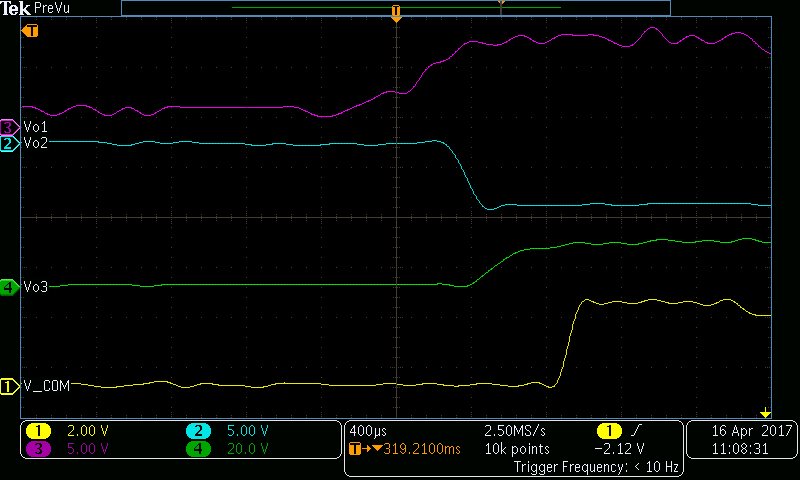
    I have taken snaps of startup ramp.

    1st waveform : VGH(Vo3)

    2nd waveform: AVDD(Vo1)

    3rd waveform: VCOM

    4th waveform: VGL(Vo2)

    Best Regards,

    Kushal Shah

  • Hello Kushal Shah,

    Thank you very much for your measurements. It is hard to see details on the top screen shot. Is it possible to increase the number of points per division on your scope to get more detail on the startup measurement?

    It seems that Vo3 is already starting when Vo1 has not reached its final value. This should not be the case. Normally Vo1 is starting first, then Vo2 and then Vo3 and they should start in a row.

    I expect that all measurements are done with the panel connected, correct? If you disconnect the panel, are the outputs starting then properly?

    Best regards,
    Brigitte 

  • Hello,

    Please see below updated image. Here we can clearly see as you say Vo1 is starting first then Vo2. 

    Regarding the panel connection, no, readings are taken without panel connection. 

  • Hello Kushal Shah,

    Please check the following:

    1. Disconnect the panel and check if the outputs are then ok.

    2. Measure as above the moment when the outputs shut down after startup. It might be possible to check why the protection of the IC is triggered.

    Another possibility would be to use TPS65101 for tests. This is the same device with higher current limit on the boost and no protection. It would be possible to find out which output triggers the protection by the use of this device.

    Best regards,

    Brigitte

  • Hello,

    I got the output. There was some connection problem in 40 PIN ffc/fpc cable used for input supply. After replacement with new cable, all outputs are OK. 

    Thank you for your support. 

    Regards,

    Kushal Shah