This thread has been locked.

If you have a related question, please click the "Ask a related question" button in the top right corner. The newly created question will be automatically linked to this question.

TPS92512 operation and reliability

Other Parts Discussed in Thread: TPS92512, LM3409, LM3401, TPS92512HV

Hi All,

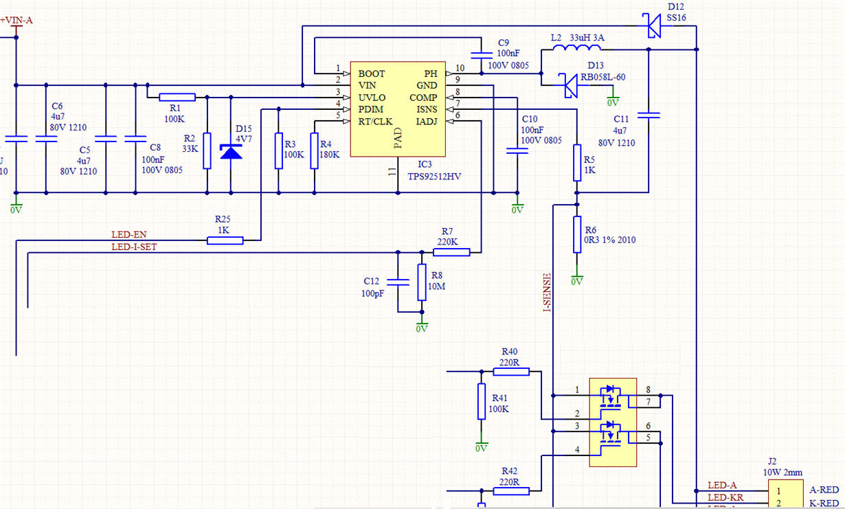
I'm considering to use a TPS92512 chip to switch it's output to one of three LED branches of different colours (R,G,B) and run a current of 850mA~1A through it.

Schematic is attached. Vo is connected to three branches of LEDs with 3 high power LEDs in each branch in series (7.5 to 11V forward voltage depending on colour) but each branch has a Mosfet switch to ensure only one branch is ON at any time. Current level can be controlled through Analog Iadj pin.

Two concerns I have is:

1. If Vin falls close to total forward voltage of LEDs, driver goes out of regulation. What behavior it will have in terms of how much current it will push through LEDs in that mode? Would Iadj pin be in charge of controlling output current when chip is not regulating? How about PDIM input?

VIN shuold be high enough to drive LEDs but if for some reason (drooping, running below rec spec) it was not, I would like a dimmed and safe operation to ensure LEDs or chip itself not damaged.

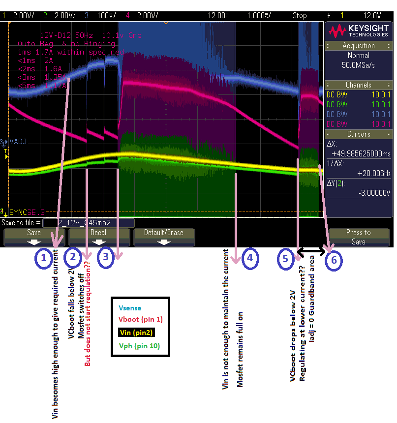
2. When Vin falls below certain level,  I see periodic negative spikes on PH pin until VIN rises to above a certain level and regulation resumes. Apparently Cboot falls below 2 V:

(Red: Boot, Yellow Vin, Green Vo,Blue Vsense)

Could these pulses be resulting in EMC issues?

3. Accidentally noticed if RT/CLK pin is touched by finger (discharged by touching Ground beforehand) chip blows up in less than a second!!!

Well although this cant happen in normal operation but wondering why is this happening. I can consistently blow up as many chips as I want by this.

I would appreciate any comments.

Thanks

Matt

  • For some reason I cannot see the pictures attached. In any case if I'm thinking of the right thing the part is operating normally. It really isn't the best part for very high duty cycle operation as what it will do if the input dips too low the part will try to go into 100% duty cycle mode and it will. But in this mode there is no way to replenish the Cboot cap so it will dishcharge below its UVLO threshold. When the output falls far enough to charge the boot cap it will restart. IADJ is still trying to regulate so it will not let it go out of control and damage the circuit or LEDs, but it could cause the LEDs to flash. I doubt it would be an EMC concern at those frequencies. As for the PH pin going negative, the power diode should prevent a large enough negative voltage to damage the device. Yes, the RT/CLK pin is known to be sensitive. I have not seen it do damage, but my lab conditions may just be different. If you really need to perform at the lower input voltage without these issues you may want to consider the LM3409 or LM3401 as they are designed to operate up to 100% duty cycle continuously if needed.
  • Thanks for reply and pictures attached for more details.
  • So my thinking was correct, that is what is happening. The LM3401 or LM3409 is much better suited and both are very robust.
  • Thanks Clinton, I had a look at LM3409 and had a few things in my mind if I could get your thoughts on.

    I'm sort of trying to figure out pros and cons of each and decide to replace LM3409 with TPS92512 or not.

    0. In the attached CRO capture of TPS92512 behaviour, I'm wondering what makes the chip go out of regulation at point 4? Why doesnt it start regulation at point 2? whats the logic behind start/stop of regulation?

    1. Re the two devices (TPs9512 vs LM3409) when the Vin – Vout Voltage drops to say ~ 2V, would you consider the TPS92512 behaviour and its mode of operation to be less guaranteed in terms of either high peak currents to the LEDS or damage to the IC if it stays in this low input voltage mode or would it be similar to the LM3409. Is either more prone to damage at low drop out voltages. This questions relates to the TPS92512’s use of a boot capacitor vs the LM3409’s internal regulator.

    2. When the power supply chip is out of regultion because of Vin falling to drop out level, what determines the current limit across LEDs? is the cip still in control of current or we should check it with ohms law?

    3. Re the oscillator sensitivity mentioned (TPS92512)– is there anything we could do on-board to make this a more robust input – eg addition of a ground plane area or earth guard ring or other around oscillator pins.

    4. I noticed in app note of LM3409 inductoe is directly connected to LED branch and there is no output cap. Now considering a situation that we turn all LED branches off (e.g. flashing) then what happens to incductance current? should we disable power supply first then turn off LED branch switch?

    I appreciate if you share any thoughts you may have.
    Thanks
    Matt
  • 0. If the input voltage is too low you will get a race condition between Vin drooping and Cboot charging and discharging. So there really is no real regulation overall. It would become a little more predictable with more input capacitance to prevent the input voltage droops.

    1. This would not damage the TPS92512 and the IC would not allow the current to exceed the regulation set point so the LEDs would not be damaged. With such low input voltage it would be basically impossible to overcurrent the LEDs unless there was a short from Vin to PH or the output. The LM3409 was designed for 100% duty cycle so it will just turn the switch full on when the input gets low, but it will stay full on since it doesn't need bootstrapping. So there will be no oscillations or flickering, the LEDs will just light up with whatever current they do at Vin - Vswitch.

    2. See #1, you can't overcurrent the LEDs if the input is so low. But neither regulator will allow the current to go above its regulation set point anyway.

    3. You could add a small capacitor like 220pF which would provide some immunity. But in reality if you just connect the RT resistor very close to the part you shouldn't have any issues. I'm not familiar with earth guard rings.

    4. The inductor (and LED) current will simply ramp down to zero when EN PWM dimming (or just turning off). If you are shunt FET dimming the inductor current just continues to run through the shunt FET so that the LED current rise time is very fast when the FET is turned off.


  • Thanks Clinton,

    The only question remains here in regards to when it's on full duty cycle, how come the current is limited and controlled? I would have thought in that mode, Mosfet is ON and Vo=Vin. If so the LED current would depend on Vin-Vmosfet-VF_LEDs-Vsense/Rsense. Assumiing Vin 12 and VF for 3 LED 10.5V and Vsense 0.1v then the Led current might go up to a few amps no matter if we have set average LED current to 1A. Is this right? HOw would the current be limited in this mode is something I cant get my head around it. Obviously when in regulation, it'll give regulated 1A current out.

    Matt
  • The reason they go into 100% duty cycle mode is because the drop across the FET is enough that there isn't enough voltage across the LED string to get the full current. The IC is still monitoring the current and if it gets sufficiently high it will start switching again to prevent it from going above regulation.

  • Hi Clinton,

    Hope you are doing very well.

    A you may recall we had a few chats before on operation of TPS92512 and our prototype is based on this.

    As a brief, I'm running 3 mutually exclusive R,G,B branches of LEDs (3 on each branch and a mosfet switch to control each branch) sharing a 0.3 ohm current  sense resistor. Various shade of colours can be generated using different proportion of R,G,B by switching from one to other within a time period. A problem rises here is when switching from Green to Red as Red forward voltage is lower than Green/Blue leaving a suddon 2-3Volt above Vf of Red on the branch which means a large overcurrent at that point until LED power supply controls situation and output drops to Vf of red and adapts and current is back to set point. This takes a bit of time which is beyond operating conditions specified in LED datasheet.

    As a possible solution I'm thinking of an interim blanking period between Green/Blue and Red to let the driver chip output voltage to drop (discharge through a branch)  before switching to red.

    This can be done either through PDIM (PWM Dimming) input Or analog Vadj. According to datasheet Vadj cannot drop LED output current to zero and there is a minimum current (30-40mV Vsense ~ about 120mA) which is not desirable as I don't want any beam of light during blanking period and I dont want to have a dummy load to consume that current. PDIM on the other hand is able to drop the current to 0 and works very well at normal operating conditions when Vin is high enough. Now, based on earlier chats about non-ideal operation of this driver in lower input Vin (when close to Vo), my question is:

    1. What is the behaviour of the driver and controlability of output through PDIM when chip goes out of regulation?

    2. Is PDIM usable reliably only at higher Vin levels or we should expect reliable operation otherwise?

    3. Apart from two above methods, are there any other options to drop the outpput current of the chip to 0? (internal/external)

    4. As a separate question, is it normal in switching driver circuits to get a bit of buzz sound from inductor? Waht causes that and how it can be reduced?

    I'd appreciate if you could share your comments. This is urgent to me at this point and thanks a lot in advance.

    Regards,

    Matt

  • Regarding the first part you could add a resistance in series with the red LED to make up the voltage difference. That would eliminate the overcurrent. Also, with analog dimming you can drive IADJ all the way to zero. But there is a +/-10mV offset in the error amplifier (realistically closer to +/-5mV) so when IADJ is zero some parts will turn off and some could still have 10mV of current sense. So that might be easier to consider a bleeder. To answer your other questions:

    1. In dropout the regulator will turn it's switch on fully until the boot cap discharges. Then it will restart switching to charge boot and then repeat the cycle. It will do the same during PWM dimming. It will still turn on and off with PDIM as you expect but the LED current will oscillate when on.

    2. It is generally reliable as long as you do not enter dropout, but it can limit the minimum duty cycle during PWM dimming. When PDIM is low boot will discharge over time. If there is very little headroom between Vin and Vout then during the off cycle boot will discharge from a Vin-Vout voltage and could hit UVLO during the cycle. That will cause the next on cycle to be messy. But if you have at least 4V differential you can dim pretty low. If you have at least 7V potential difference boot can charge fully and you can dim as low as you like.

    3. A bleeder is generally the easiest way if you need to ensure zero current. Pulling UVLO low will also give you zero current, but if COMP discharges below 0.7V while UVLO is low then next time UVLO is pulled high the part will go through a normal startup sequence. Maybe that is not a problem for your application.

    4. It's common to have inductors and ceramic capacitors buzz when PWM dimming at an audible frequency. With inductors generally just changing the case size, type, and/or manufacturer will work. It can also be potted if necessary. The same goes for ceramic caps. Often just changing the case size will work and/or use multiples (swap a 1210 capacitor to two 1206 capacitors, this also halves the rms current in each). Some companies also have a line of low audible noise ceramics.

  • Hi,

    A different query but still on TPS92512.

    My query is about field failure rate of TPS92512/TPS92512HV and thermal shutdown functionality.

    I have a few failed units diagnosis being the output PH pin has a low resistance to the ground (1~20 ohms) which indicates power MOSFET has gone short circuit. Failed units are usually fail in early stages of usage. Flyback diode and a protection TVS (D12) on output (revised to be parallel to C11) are not damaged (when tested of the circuit). 
     
    I was wondering what event could cause TPS92512 fail in a number of units whilst many others working OK for a long time.
    1. If we blame poor slug/pad soldering on a few units causing poor thermal interface of the chip to ground plane, hence higher operating temperature, could that be the root cause? If so, why the thermal shutdown on the chip does not protect it?
    2. If not temperature, any idea what could cause this kind of damage?
    3. Is there any data on failure rate of TPS92512 from TI? (assuming no design error)

    I know TPS92512 is not an ideal choice for 100% duty cycle but I don't this the application type would be the cause of failures.
    I appreciate if you share your thoughts or suggest tests to help find the root cause.

    Matt

  • Hello Matt,

    Is there any way you could share your layout? A poor DAP connection alone could do it for two reasons: The first is if there is little to no connection the thermal overshoot before thermal protection kicks in might cause damage (unlikely but possible in some cases). The second is that if it isn't fully electrically connected (or a high resistance connection) there will be a lot of noise generated and pins can be over-voltaged and/or see negative voltages, both of which can cause damage. This might be your case.

    If not then the layout would be the next thing to look at. If the ground connections aren't very good or the routing is not very good you could see significant negative spiking on the PH pin regardless of the diode and that could damage the switch. I would be happy to look over your layout and comment if you want to provide it.

    Regards,

    Clint

  • TPS92512_Layout B.zipTPS92512_Layout A.zipSorry if my response is duplicating, for some reason I don't see my reply I sent earlier this morning. I thought it might not posted .

    Hi Clint and thanks very much for response.

    Good point on PAD connection to Gnd and it's effect on thermal performance and also noise susceptibility.

    The datasheet says voltage difference on the PAD should be within +/-200mv versus Gnd. If no solder paste or any problem that might be an issue.

    On the layout, I have attached two layouts I have and appreciate any thoughts specially on layout A.

    Matt

  • Hello Matt,

    The B version seems to be better overall. If you were to rotate the input capacitors so that their grounds tied directly to the grounds of the IC and the current sense resistor it would be pretty good. I would also not have a fill for the current sense trace as that could give you much more area for noise coupling. I would run a single trace to the IC and a single trace to your other current sense circuitry.

    The A version looks a bit more problematic. I love your liberal use of ground vias, I always recommend that where possible. But the placement of the grounds could for sure give you some ground errors and spiking on the switch edges. Refer to the layout section of the datasheet. But basically the critical ground locations are the input capacitors, the IC/DAP, the rectifier diode, and the current sense resistor. In this version they are somewhat far apart and again especially the input caps are a ways away. Ideally you tie these grounds as close together as possible, preferably with a good ground plane with plenty of vias like you are doing. You want the switching current loops as small as possible and their ground current return paths as small as possible as well. As it is there are some sizeable loops. On top of that you are running a high impedance current sense trace right near the switching diode and its ground return path so there is potential for noise coupling that could cause issues. In any case I can see the possibility of voltage spikes with this layout, not that they are alll necessarily big enough to cause problems. It may be a combination of layout and not a solid enough DAP connection. Or it could simply be the devices with faster switch rise/fall times are the ones that fail due to larger spikes below ground.

    Basically layout could do it and improper DAP soldering could do it, a combination is only more likely. So I would focus on both. There are some layout guidelines in the datasheet and some layout app notes on ti.com. It really helps, a good portion of problems are due to layout. But soldering the DAP sufficiently is also key for almost all devices that have a DAP.

    Regards,

    Clint

  • Thanks so much Clint!

    I'm now looking for a test or monitoring method to check some sample units to see if I can find any negative spikes. Obviously these can not be faulty units and can only check working units.
    I would probably set up CRO on single shot with trigger on a negative value.
    If you know of a better method I'd appreciate your thoughts.

    Are you aware of any effective way to examine soldering quality of DAP on the failed units?

    Thanks
    Matt
  • Hello Matt,

    Yeah, it can be hard. You kind of have to catch one when it fails and that is difficult without many iterations, but a "better" board may show borderline spiking that could give you some idea since you know there will be variations from board to board.

    As for the quality of the DAP the only way I am aware of (and I have not done it myself, some other group does it) is with x-ray. You can see dark patches where the DAP and PCB connect and it will be much lighter where they do not. I'm not sure if you have this capability or not and I'm not sure who does. But there are probably labs that could do it if you don't. Maybe whoever did the board assembly does. I have seen more than one case where the assembly process has had to be tweaked to get proper DAP seatin.

    Regards,

    Clint

  • Thanks Clint!

    I have captured something interesting happening on V_PH (hence V_Boot) when V_adj input is 0V. It's happening on Type A board (scope_4.bmp) and to a lesser degree on Type B (scope_23.bmp). The reason it's interesting is that one would expect only switch On/Off during regulation mode and when boot cap has at least 5V across it. Whilst, as shown in attached snapshots (V_PH_waveforms.zip), there is a sine shaped component happening too. I'm interested to know how is that coming about. During that time LED current is about 90-100mA. Cursors measure switching frequency which is under 580KHz.

    Any thoughts?

    Also I have a question on the circuit symbol on gate of the high-side MOSFET in the controller block diagram. I'm wondering what that component is? is it a tri-state buffer? What's the function?

    Thanks so much.

    Matt

  • Hello Matt,

    The ringing you are seeing in the switch waveform is normal. All it means is that the inductor/LED current is low enough that you are in discontinuous conduction mode (DCM). That means the inductor current is dropping to zero each switch off cycle. When it hits zero the diode stops conducting and the inductor rings against its parasitic capacitance. You will see this in all switching regulators when you enter DCM. So naturally you will enter DCM earlier with a lower L value and later with a higher L value.

    All that is that's connected to the gate of the FET is a buffer/gate driver. The logic cannot supply enough current to drive the gate by itself or pull the gate above PH which is what the boot cap/buffer combination is for.

    Regards,

    Clint

  • Hi Clint,

    Thanks for your reply.

    Yes as you clarified the ringing effect is normal. That ringing is happening at the time of switch on and switch offs and has a higher frequency and is damped.

    However, the one I was mainly interested to have your thoughts on is the one highlighted in scope_4.bmp which is one bell-shaped waveform happening before switching (and ringing). Its width is almost same as switching pulse itself and its amplitude can be as high as PH itself. I don't see this when Vadj is 1.8V (full brightness).

    I'm considering this as a separate phenamenon, but do you think this is same as ringing or a part of it?

    Thanks

    Matt

  • Hello Matt,

    Yes, what you are seeing in scope shot 4 is exactly what I am talking about. It doesn't happen at full brightness because the inductor current stays continuous (does not drop to zero) at the higher LED current. It is normal.

    Regards,

    Clint

  • Hi Clint,

    I have been working on this on and off and waiting for some samples worth taking to X-Ray.

    Finally I got 2-3 faulty samples (XRAY_defect.zip) and took them along with a few working ones (XRAY_OK.zip).

    It was very interesting to see the X-Ray images of an IC for the fist time, specially seeing wire bounds from pins to inside.

    In all faulty ones the three wire bounds from Pin 2 (Vin) are broken which I thought it's a pattern.

    It was aligned with the visual symptom I was seeing which was a damage on package around Pin2 and Pin 3.

    Now my questions are:

    1. Does this mean anything or not? possibly pointing to cause of failure.

    2. How does DAP soldering look like in terms of quality? Are they satisfactorily or better to improve or urgently need to be improved?

    I'd appreciate any thoughts.

    Matt

    Attachments:

    XRAY_defect.zip

    XRAY_OK.zip

  • Hello Matt,

    Those are some good pics. To answer your questions:

    1. Yes. Blown bond wires are always due to an overcurrent event, or a series of overcurrent events over time. It could be from PH getting pulled below ground or from shorting PH or the output to ground. But you can say for sure it is an overcurrent event of some sort.

    2. The DAP soldering looks like it's probably ok. Ideally it spreads from edge to edge both ways, but at least you know you have some decent contact. The dark blobby areas you see are what are soldered down and the lighter areas around the blob are where the DAP does not make contact.

    Are those recent failures? Did they happen quickly or over time? Did you update the layout and then they still happened?

    By the way, I will be out for a couple of weeks after today on vacation, so my responses may be delayed. If you need anything and I will not have time to take care of it (I will check in periodically) I will pass it on to somebody who can help.

    Regards,

    Clint